KayO
Purdue, ECE 477 senior design
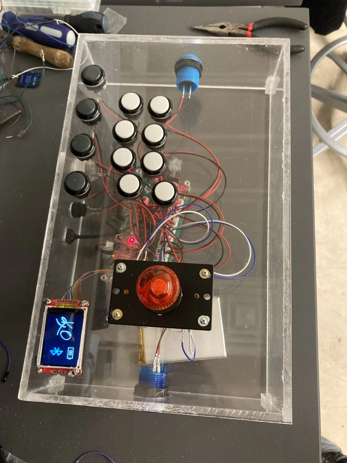
The main board of a fight-stick game controller that runs from a Li-Po cell or USB. The built board passed every check at the course demo.
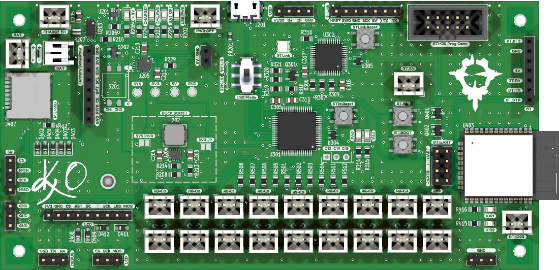
- Fuel gaugeBQ27441
- Micro-USBPower and data
- STM32F411Main MCU
- On-board ST-LinkSTM32F103
- Buck-boostTPS63802, 3.3 V
- 18 button inputsJST connectors
- ESP32-WROOM-32EBluetooth
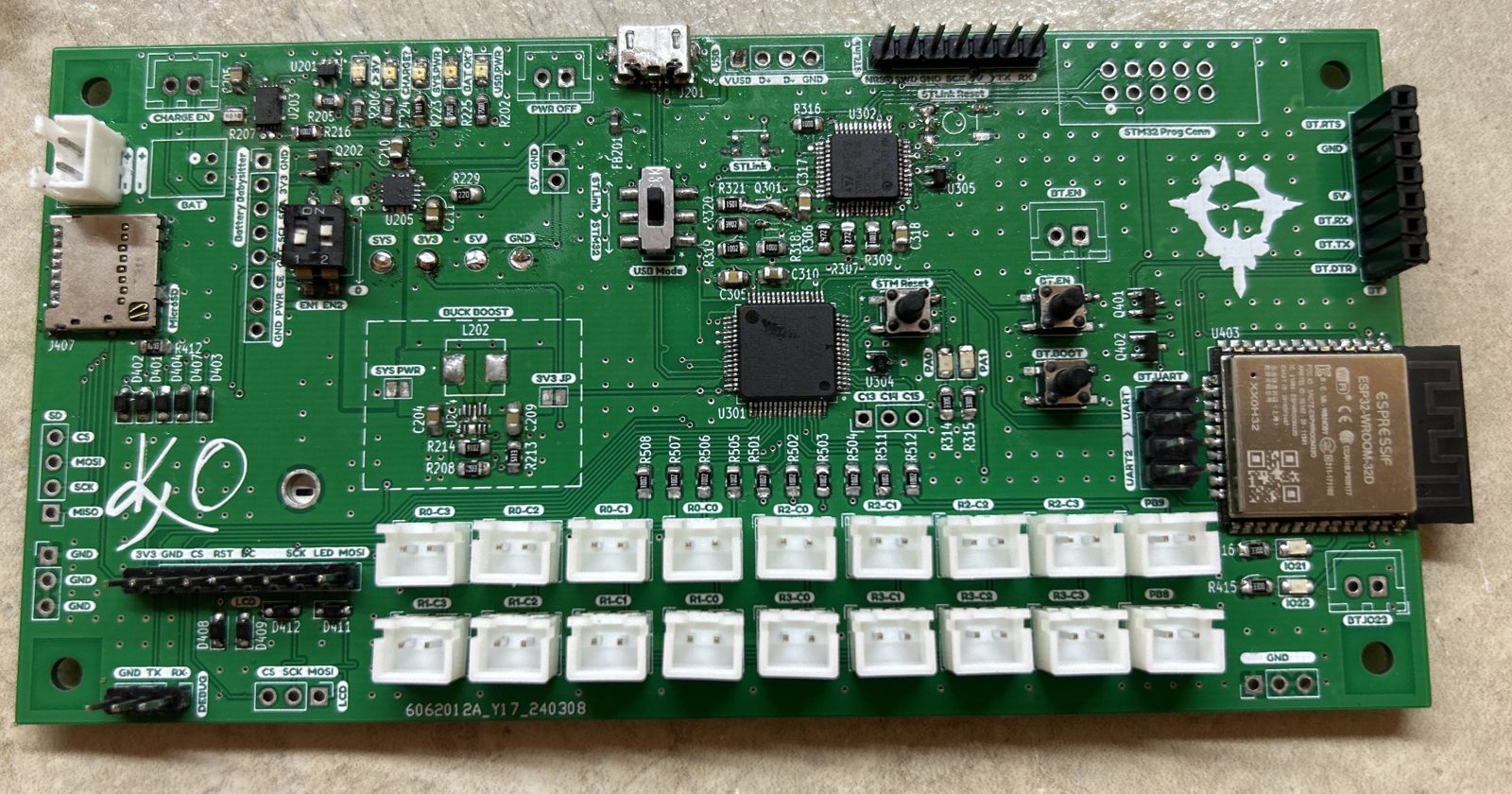
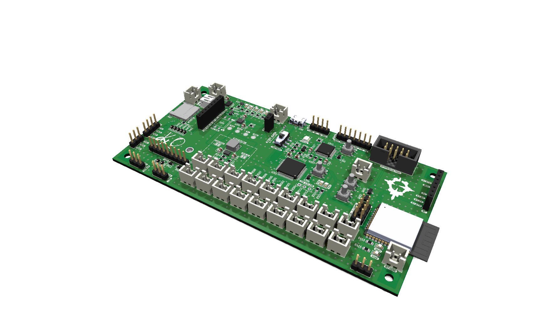
140 × 70 mm2 copper layers213 footprints209 nets569 viasFabricated March 2024
- Power
- Logic
- I/O
- Sensing
The problem
KayO is an arcade fight stick: a joystick and buttons that play games over USB or Bluetooth. My team of four built it in ECE 477, Purdue’s senior design course, and I designed its main board.
The board had to read 18 button inputs, run from one Li-Po cell or from USB, and charge the cell. Our power budget put the system at about 550 mA at 3.3 V, so the converter had to supply 800 mA. We had twelve weeks from the first sketch to the demo, and I would solder every part by hand.
How it works
The board turns USB or a Li-Po cell into one 3.3 V rail, reads 18 buttons, and sends them to a computer over USB or Bluetooth.
The power blocks sit in the top rows: a charger, a fuel gauge and a buck-boost converter. Below them, an STM32F411 microcontroller reads the buttons and acts as a USB game controller, an ESP32 module carries Bluetooth, and an on-board ST-Link programs the STM32. Click a block to see what it does and why I chose it.
KayO main board, block by block. Blocks: Li-Po cell (one cell); Charger (BQ24075); Micro-USB (power and data); Fuel gauge (BQ27441); Buck-boost (TPS63802, 3.3 V); USB switch; ST-Link (STM32F103); STM32F411 (main MCU); Buttons (18 inputs); LCD (TFT screen); microSD (card socket); ESP32 (Bluetooth). Li-Po cell to and from Charger; Micro-USB to Charger, 5 V; Charger to Buck-boost; Buck-boost to STM32F411, 3.3 V; Micro-USB to and from USB switch, USB; USB switch to and from STM32F411, USB; USB switch to and from ST-Link, USB; ST-Link to STM32F411, SWD; Fuel gauge to and from STM32F411, I2C; Buttons to STM32F411; STM32F411 to LCD, SPI; STM32F411 to and from microSD, SPI; STM32F411 to ESP32, UART.
Click a labeled block to see what it does and why.
The board, block by block
Power is in the top rows, and the STM32F411 below them reads the buttons and talks to everything else. Click a block to see what it does and why I designed it that way.
In this layer
- Micro-USB The board's one USB port: 5 V for the charger, and data for the game controller or the programmer.
- Charger A BQ24075 runs the board from USB when it is plugged in, from the Li-Po cell when it is not, and charges the cell.
- Fuel gauge A BQ27441 fuel gauge, a chip that tracks the charge going into and out of the cell, reports the cell's state to the STM32F411 over I2C.
- Buck-boost A TPS63802 buck-boost converter, a switching regulator that can step a voltage down or up, makes the 3.3 V rail.
- ST-Link An STM32F103 circuit that loads firmware into the STM32F411 over SWD, its debug interface, through the same USB cable.
- STM32F411 The main microcontroller. It reads the 18 buttons and acts as a USB game controller to the computer.
- ESP32 An ESP32-WROOM-32E module carries Bluetooth. It gets the button states from the STM32F411 over a serial link.
- Buttons The joystick and buttons plug into 18 JST connectors. Sixteen share a 4 × 4 matrix, and two have their own pins.
- LCD A header for the TFT LCD used in the ECE 362 course, driven by the STM32F411 over SPI.
- microSD A microSD socket on its own SPI bus from the STM32F411, with a card-detect line. The card holds the bitmap images the LCD shows.
Micro-USB: power and data in one port
The board's one USB port: 5 V for the charger, and data for the game controller or the programmer.
I chose micro-USB over USB-C because it is easier to solder by hand, and I soldered every part on this board.
One port, two chips
A slide switch sends the data lines either to the STM32F411, which acts as the game controller, or to the on-board ST-Link that programs it.
Protection
TVS diodes, parts that clamp a voltage spike to ground, guard both data lines and the 5 V line against static discharge.
Charger: one cell, two sources
A BQ24075 runs the board from USB when it is plugged in, from the Li-Po cell when it is not, and charges the cell.
The cell
One Li-Po cell powers the board away from a computer. Our specification set a target of about five hours on battery. It was not measured.
Status and a fallback
Three LEDs show charging, power good and system power. A header takes a SparkFun Battery Babysitter, the charger and fuel-gauge board we prototyped on, in case the on-board charger failed.
Fuel gauge: how full the cell is
A BQ27441 fuel gauge, a chip that tracks the charge going into and out of the cell, reports the cell's state to the STM32F411 over I2C.
Result
It was one of the five functions checked at the course demo, and it worked.
Buck-boost: 3.3 V from either source
A TPS63802 buck-boost converter, a switching regulator that can step a voltage down or up, makes the 3.3 V rail.
USB gives 5 V and a Li-Po sags below 3.3 V as it empties, so one converter had to step down from one source and up from the other.
Why this part
Our power budget put the system at about 550 mA at 3.3 V, so the converter had to supply 800 mA. My home-made SEPIC, a 555 timer and a MOSFET, stepped up in simulation but would not step down. I found and compared the candidates and made the case to the team, and we chose the TPS63802 over TI's TPS63021, whose 2 A was “simply overpowered” for our 800 mA. It cost efficiency stepping down: 91 % against 95 %.
The fallback
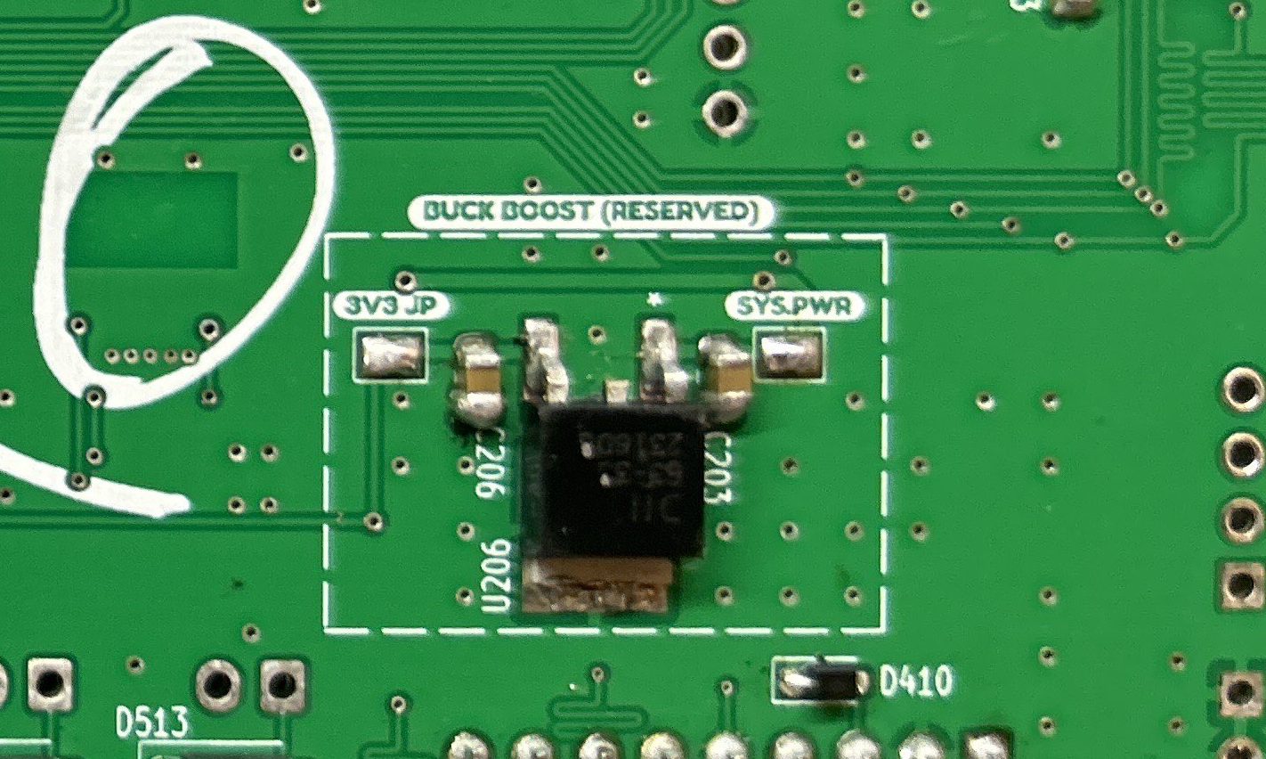
I kept a footprint for an AP7363 LDO, a linear regulator, and four solder jumpers pick which one feeds the rail. We chose an LDO over a second buck-boost because it is much simpler: the buck-boost was hand-soldered, and we wanted certainty that the board would run. It costs efficiency, because an LDO turns the voltage it drops into heat.
At bring-up
The buck-boost first gave 0.8 V. Its inductor was out of stock, and the substitute was rated for 100 kHz switching, so I ran the board on the LDO. On a blank board the TPS63802 later held 3.3 V from both 5 V and 2.5 V in. The load was not recorded.
Two ways to make 3.3 V
Schematic of KayO's 3.3 V supply. SYS.PWR splits into two paths. On the upper path, solder jumper JP202, bridged in copper, feeds PWR_JP to U204, a TPS63802DLAR buck-boost converter with C204 22 µF at its input, the 0.47 µH inductor L202 across its L1 and L2 pins, C209 22 µF at its output, and the R213 511 kΩ and R214 91 kΩ divider from its output to its FB pin. Its output, 3V_JP, reaches the 3.3 V rail through JP204, also bridged. On the lower path, open solder jumper JP201 feeds U206, an AP7363-33D-13 LDO regulator with C203 10 µF at its input and C206 10 µF at its output, and its output reaches the 3.3 V rail through JP203, also open. Connections: SYS.PWR joins JP202, JP201; PWR_JP joins JP202, C204, U204 VIN; 3V_JP joins U204 VOUT, C209, R213, JP204; FB joins U204 FB, R213, R214; +3V3 joins JP204, JP203; GND joins C204, U204 GND, C209, R214, C203, U206 GND, C206; (unnamed) joins U204 L1, L202; (unnamed) joins U204 L2, L202; (unnamed) joins JP201, C203, U206 IN; (unnamed) joins U206 OUT, C206, JP203.
The board's 3.3 V supply, with parts, values and connections from the PSU schematic sheet. SYS.PWR is the output of the BQ24075 charger, which runs the board from USB or the Li-Po cell. Four solder jumpers pick which regulator feeds the 3.3 V rail.
- JP202 and JP204 are bridged in copper, so the TPS63802 buck-boost feeds the 3.3 V rail. It steps USB's 5 V down and lifts a Li-Po that has sagged below 3.3 V.
- R213 and R214 divide the output back to U204's FB pin, which sets the 3.3 V.
- JP201 and JP203 are open, and U206 sits on a reserved footprint. Cutting JP202 and JP204 and bridging JP201 and JP203 moves the rail to the LDO.
- The LDO is much simpler. We gave up efficiency for certainty, because the buck-boost was hand-soldered and might need a fallback. On the first board the buck-boost gave 0.8 V, and the board ran on the LDO.
As built, JP202 and JP204 are bridged in copper and JP201 and JP203 are open. Left out: U204's EN pin (tied to its input), its MODE and PG pins with the PG pull-up R208, and the rest of the charger.
Numbers
| At 3.3 V and 800 mA | Stepping down | Stepping up |
|---|---|---|
| TPS63802 (chosen) | 91 % | 91 % |
| TPS63021 | 95 % | 88 % |
| TPS63031 | 90 % | 80 % |
ST-Link: a programmer on the board
An STM32F103 circuit that loads firmware into the STM32F411 over SWD, its debug interface, through the same USB cable.
I put it on the board for “a more convenient way of programming”: one cable, no separate programmer.
Where it came from
I based it on the ECE 362 course's programmer stick, an STM32F103 board, and drew its circuit into KayO's schematic.
The USB switch
A slide switch sends the port's data lines to the ST-Link for programming, or to the STM32F411 for play.
Fewer moving parts
In the second layout I replaced a switch on its debug lines with a header, to “reduce the risk of malfunction”.
STM32F411: the controller
The main microcontroller. It reads the 18 buttons and acts as a USB game controller to the computer.
Every other block reports to it or takes orders from it: the fuel gauge, the ESP32, the LCD and the microSD socket.
Clocks
Both STM32s take their clock from MAX7375 silicon oscillators instead of crystals, on the instructor's recommendation: “more compact … and way easier to solder”.
At bring-up
Flux corroded untented vias, vias left bare of solder mask, under the STM32F411, even after an alcohol clean. We built a fresh board instead of fly-wiring it. The final file still leaves its vias untented, because no revision followed.
Firmware
The firmware on it is the team's work, not mine.
ESP32: Bluetooth
An ESP32-WROOM-32E module carries Bluetooth. It gets the button states from the STM32F411 over a serial link.
We chose it over the RN42 Bluetooth module, which “is not working due to the incompatibility in Bluetooth versions”, and whose Bluetooth 2.1 “causes nearly 2s delay”.
What it cost
A second microcontroller, which we had set aside in January, and a serial link from the STM32 that packs six buttons into each byte.
Programming it
Before fab I dropped its USB-to-serial chip and second USB port. It is programmed through a header instead, where two transistors let the adapter reset it into boot mode. The STM32F411 can reset it too.
At bring-up
An ESP32-WROOM-32D was fitted in place of the designed 32E. Its BOOT pull-up was one of three schematic errors I patched by hand.
Buttons: 18 inputs
The joystick and buttons plug into 18 JST connectors. Sixteen share a 4 × 4 matrix, and two have their own pins.
A matrix reads 16 buttons with 8 pins, and a diode on each button stops “ghost inputs” when several are held at once.
At bring-up
I changed the matrix resistors from 10 kΩ to 1 kΩ by hand, “so that it can sense the input better”.
LCD: a small screen
A header for the TFT LCD used in the ECE 362 course, driven by the STM32F411 over SPI.
Result
It worked at the course demo. Its header's pinout was one of three schematic errors I patched by hand at bring-up.
microSD socket
A microSD socket on its own SPI bus from the STM32F411, with a card-detect line. The card holds the bitmap images the LCD shows.
Protection
Before the order was approved, staff review asked for more ESD protection. TVS diodes went from 4 to 14, on the card's lines among others.
What the card holds
The firmware loads pictures from the card to show the battery level, the current mode, and whether USB is plugged in.
Result
It was not one of the functions checked at the demo.
Design decisions
The board went through three layouts in twelve weeks. Hand soldering shaped it: I chose micro-USB over USB-C, and 0805 passives over 0603, because both are easier to solder by hand, and the ECE shop and the course’s parts cupboard stock them. The two biggest choices are in their blocks above: the buck-boost converter and the ESP32.
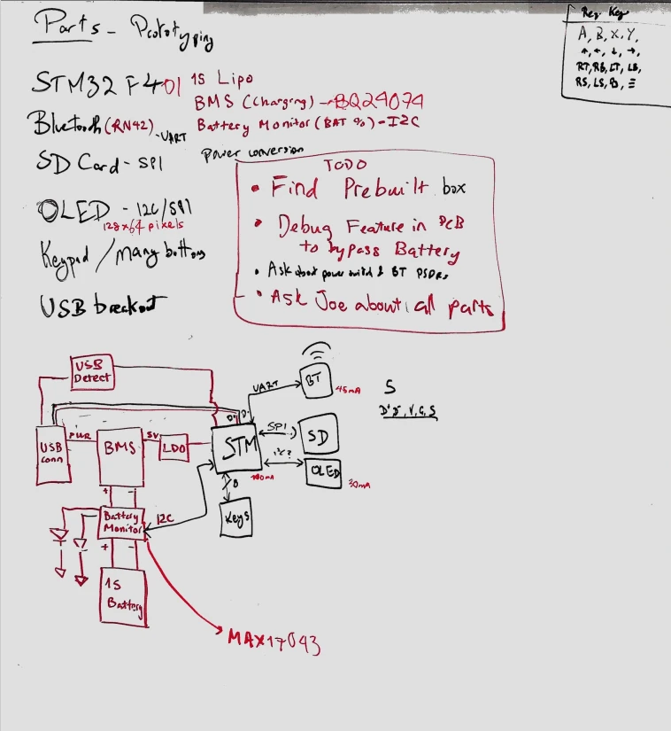
Architecture on a whiteboard
STM32F4, RN42 Bluetooth, a 1S Li-Po with charger and fuel gauge, SD card, display.
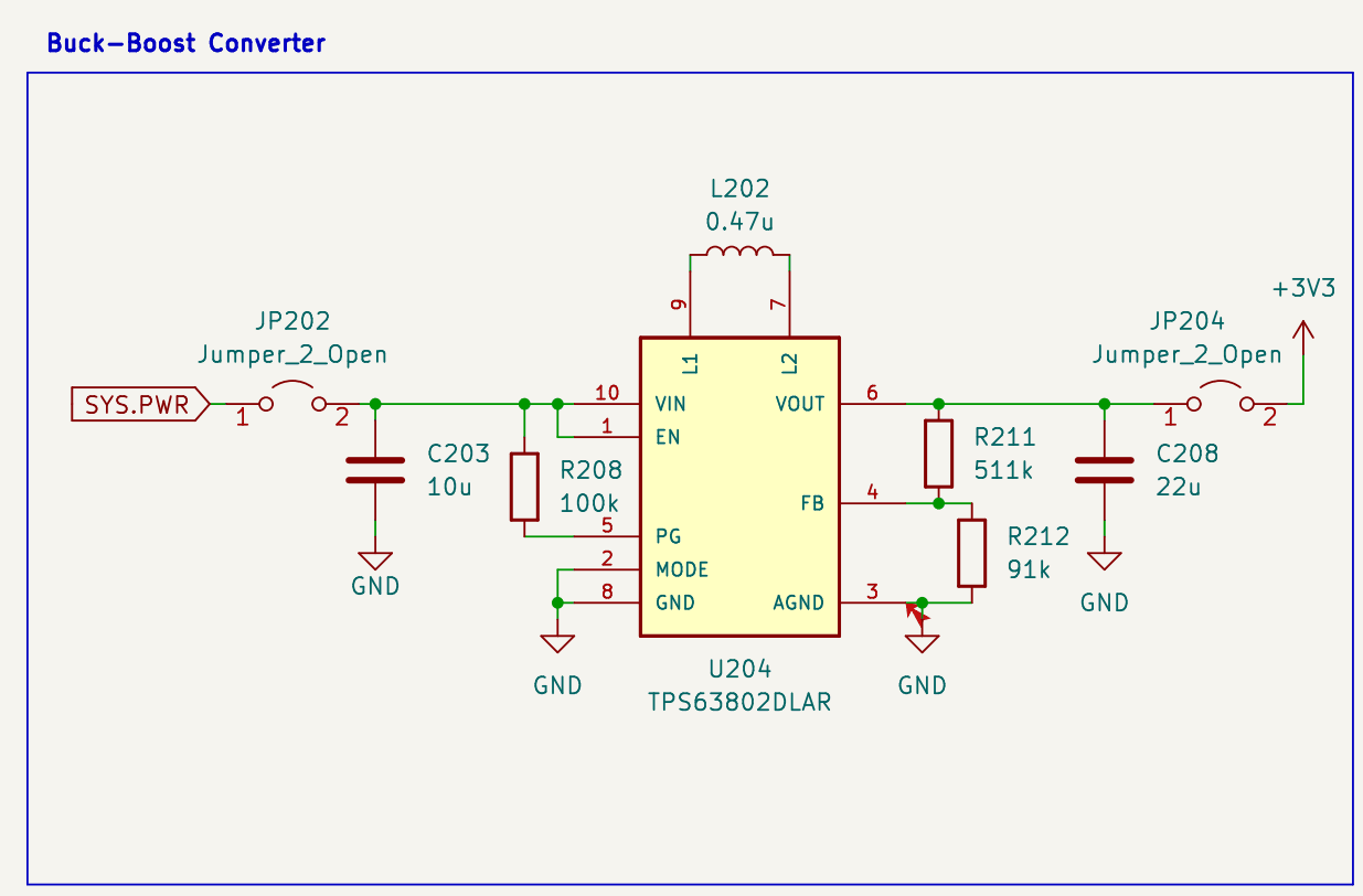
Buck-boost replaces the SEPIC
One 3.3 V rail from 5 V USB or a sagging Li-Po.
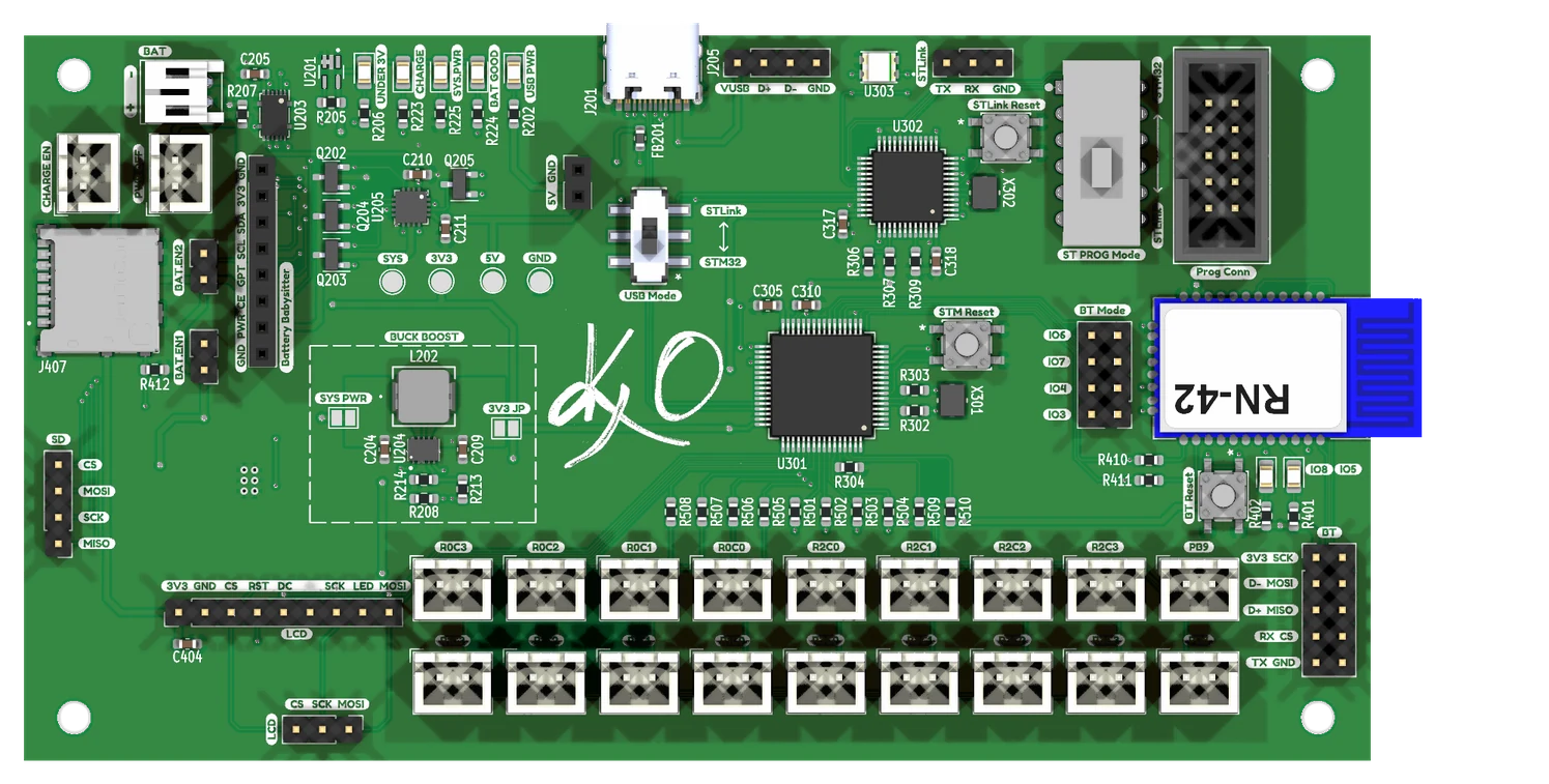
First layout
Two layers, 130 × 70 mm, 5 mil traces, RN42 antenna past the edge.
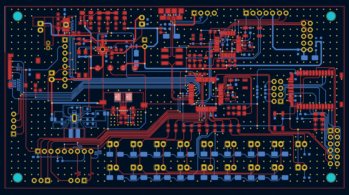
Fixed for manufacture
8 mil traces, 0.4 mm vias, silicon oscillators for crystals, ground stitching that took the board from about 200 vias to 663.
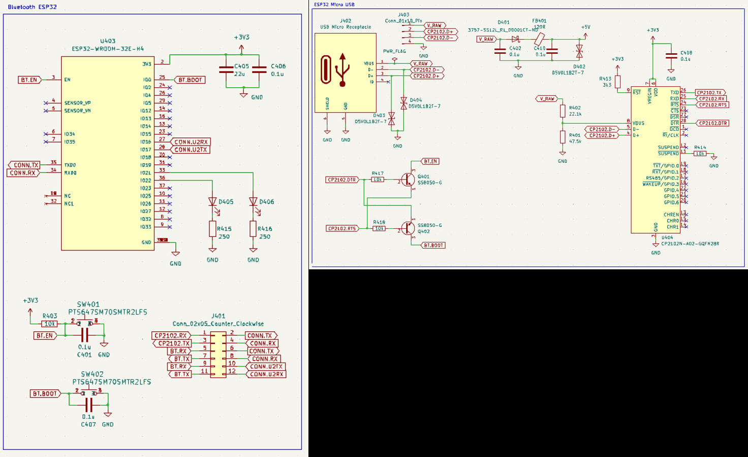
RN42 out, ESP32 in
Bluetooth moves to an ESP32 module, and the board widens to 140 mm.
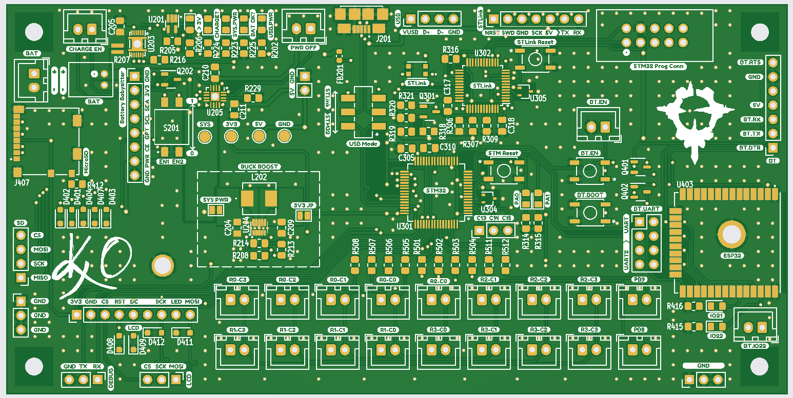
Ready for fab
0805 passives, TVS diodes up from 4 to 14, then ordered from JLCPCB.
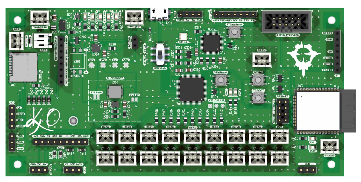
Bring-up
My first board came up on its fallback regulator, because the buck-boost’s substitute inductor was wrong. A second board replaced one whose vias flux had corroded, and I patched three schematic errors by hand. Each fix is in its block above.
Results
The board passed the course demo on 9 April 2024. USB, the link to the ESP32, the LCD, the buck-boost and the fuel gauge all worked. On a blank board the buck-boost held 3.3 V from 5 V and from 2.5 V in; the load was not recorded.
Our specification set targets of a 60 Hz report rate, under 100 ms of input lag on USB and about five hours on battery. None of them was measured.
Explore the board
Pan, zoom and click any part. The three views follow each other.
Loading the board layout.
Loading the schematic.
Credit
I designed the PCB and soldered every part. The firmware is the team’s work, and a friend drew the KO mark.