ECELabs GPIO board
ECELabs, Purdue ECE teaching labs
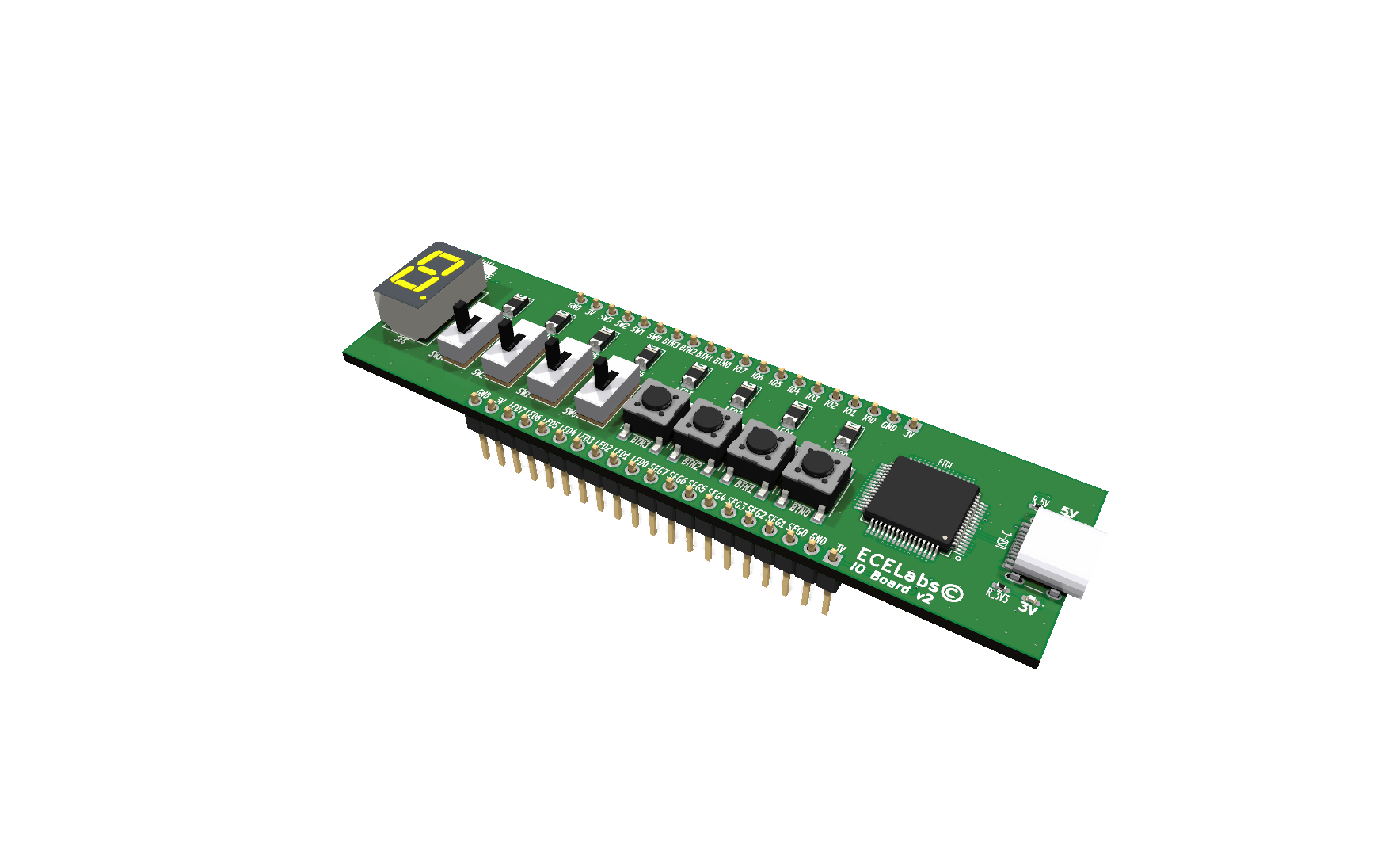
A narrow four-layer I/O board: one FT4232H puts a seven-segment display, LEDs, switches and push buttons behind a USB port. 25 were ordered assembled.
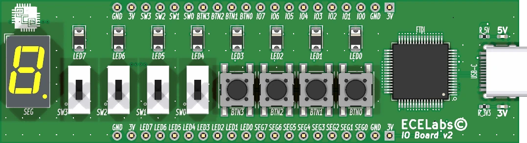
- 8 LEDs1206
- Two 1x20 headersPins out
- FT4232HLUSB interface
- HDSP-7403Seven-segment display
- 4 slide switchesInputs
- 4 push buttonsInputs
- USB-C portTo computer
92 × 25.5 mm4 copper layers85 footprints83 nets199 vias
- Logic
- I/O
- Sensing
The problem
In ECE 270, students learn to use an FPGA and logic gates and to write SystemVerilog. The lab was also building a GPIO streaming link, code that mirrors pins between a computer and a lab station over the network.
My planning diagram for this board is titled “GPIOStream”. It lists “8 GPIO (For Stream)” beside push buttons, LEDs and a seven-segment display, all reached over USB. I drew two versions in September and October 2023.
How it works
An FT4232H, a USB chip with four 8-bit ports, does all the work; the board has no processor. Each port takes one group of eight lines: general I/O for the stream, buttons and switches, LEDs, and a seven-segment display. Click a block to see what each part does.
ECELabs GPIO board v2, block by block. Blocks: Computer (over USB); USB-C (power and data); AZ1117 (5 V to 3.3 V); FT4232H (four 8-bit ports); Port A (8 I/O lines for the stream); Port B (4 buttons, 4 switches); Port C (8 LEDs); Port D (seven-segment display). Computer to and from USB-C, USB; USB-C to and from FT4232H; USB-C to AZ1117, 5 V; FT4232H to and from Port A; Port B to FT4232H; FT4232H to Port C; FT4232H to Port D.
Click a labeled block to see what it does.
The board, block by block
One FT4232H sits between the USB port and four groups of eight lines. Click a block to see what it does.
In this layer
- USB-C One USB-C port brings in 5 V and carries the FT4232H's USB data.
- AZ1117 An AZ1117 regulator makes the 3.3 V rail from the port's 5 V.
- FT4232H An FT4232H, a USB chip with four 8-bit ports, does all the work. The board has no processor.
- Port A Eight general I/O lines, IO0 to IO7, that run only to a 1×20 header.
- Port B The second port reads four push buttons and four slide switches.
- Port C The third port lights eight LEDs.
- Port D The fourth port drives the seven segments and decimal point of one HDSP-7403 display.
USB-C: the board's one cable
One USB-C port brings in 5 V and carries the FT4232H's USB data.
Before the second order
My commit of 30 October 2023 reads “Add ESD on USB and Pull up NRST”. ESD diodes clamp static discharge on a connector’s lines. The board went from one to three, on both USB data lines and the 5 V line.
AZ1117: the 3.3 V rail
An AZ1117 regulator makes the 3.3 V rail from the port's 5 V.
FT4232H: four ports, no processor
An FT4232H, a USB chip with four 8-bit ports, does all the work. The board has no processor.
A program on the computer sets and reads the ports over USB, each port taking one group of eight lines.
Pins out
All 32 lines also run to two 1×20 headers.
Before the second order
The same commit added a 10 kΩ pull-up that holds the FT4232H’s reset pin high, its inactive state. The commit does not say what failed on the first boards.
Port A: lines for the stream
Eight general I/O lines, IO0 to IO7, that run only to a 1×20 header.
My planning diagram lists them as “8 GPIO (For Stream)”.
Port B: buttons and switches
The second port reads four push buttons and four slide switches.
Port C: LEDs
The third port lights eight LEDs.
Port D: the display
The fourth port drives the seven segments and decimal point of one HDSP-7403 display.
Design decisions
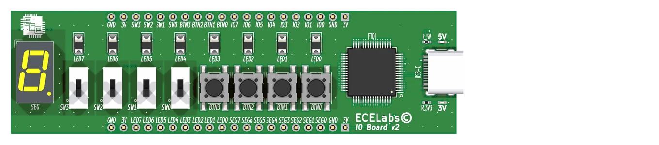
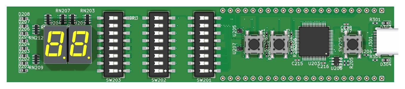
Version 2 is 38 mm shorter than version 1 and has no level shifters, the chips that translate signals between two supply voltages. Version 1 had seven, with a direction line for each pin.
Bring-up
JLCPCB invoices show 15 assembled v2 boards ordered on 6 October 2023. I changed the design before the second order, of 10 boards on 6 November. The two changes are in the USB-C and FT4232H blocks above.
Results
25 assembled v2 boards were ordered in all. I found no order for version 1. No test of either version is on record, so nothing on this page is measured. The I2C carrier and the software are the other parts of the lab’s system.
Explore the board
Pan, zoom and click any part. The schematic opens on the FTDI sheet, where the FT4232H is.
Loading the board layout.
Loading the schematic.
Credit
I designed both versions of the board.