SoCET AFTx05 test board
Purdue, SoCET VIP team
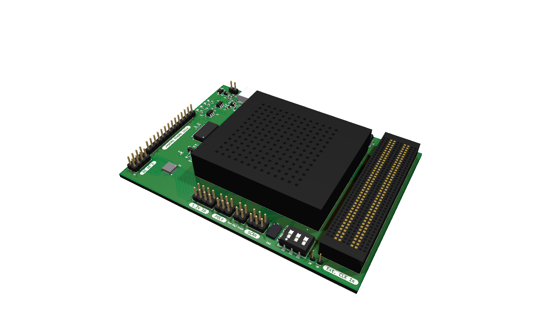
A four-layer test board that joins Purdue SoCET's AFTx05 chip to an FPGA board. It was fabricated, and not fully tested.
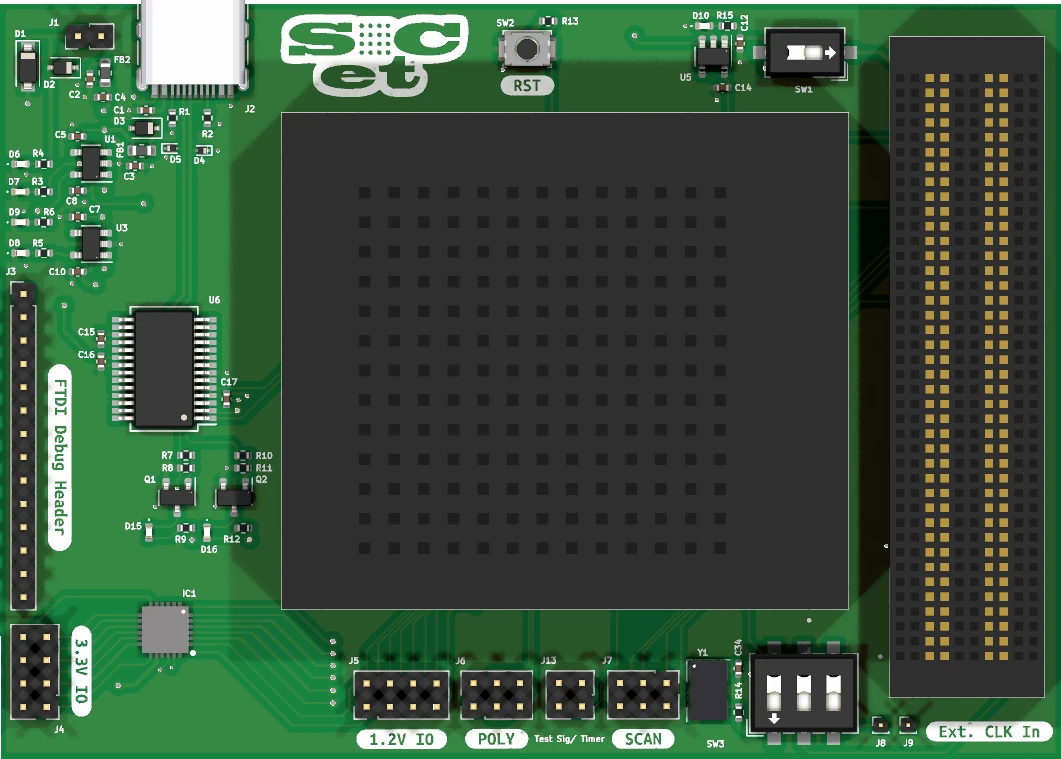
- AFTx05 footprintChip under test
- AP2112K LDO5 V to 1.2 V
- GPIO header3.3 V, 2x4
- FT232RLUSB to UART
- Clock select3-way DIP
- FMC connectorTo FPGA board
90.9 × 64.7 mm4 copper layers105 footprints180 nets199 vias15 test points
- Power
- Logic
- I/O
- Sensing
The problem
SoCET is a chip-design team in Purdue’s Vertically Integrated Projects (VIP) program, and its PCB team tests each chip after it is made. The AFTx05, its fifth chip, was taped out (sent for fabrication) in Spring 2020. It runs at 1.2 V and is built around an external memory, which an FPGA provides.
The board had to join the chip to an FPGA development board. It also needed “a lot of ways and options to debug and analyze”: test points for oscilloscope probes, header rows, and more than one power input. Teams had worked on the board since 2020; by my account, mine drew its first complete schematic.
How it works
The chip sits in a footprint in the middle of the board. The board gives it power, a clock and two links: an FMC connector to an FPGA development board, and USB through an FT232RL. Click a block to see what it does and why.
AFTx05 test board, block by block. Blocks: USB-C (power, serial); Regulators (3 × AP2112K); FT232RL (USB to serial); AFTx05 (chip under test); FMC connector (to the FPGA); Test access (15 test points); Clock select (3-way DIP). USB-C to Regulators, 5 V; USB-C to and from FT232RL, USB; Regulators to AFTx05, 1.2 V; FMC connector to Regulators, 3.3 V; FT232RL to and from AFTx05, UART; AFTx05 to and from FMC connector, address, data; FMC connector to Clock select, FPGA clock; Clock select to AFTx05, CLK; AFTx05 to Test access.
Click a labeled block to see what it does and why.
The board, block by block
USB and power come in at the left, and the FPGA board plugs in at the right. Click a block to see what it does and why.
In this layer
- AFTx05 SoCET's fifth chip sits in a footprint in the middle of the board and runs at 1.2 V.
- FMC connector FMC is the standard mezzanine connector on FPGA boards. This one plugs the board into an FPGA development board.
- Regulators Three AP2112K linear regulators, which drop the extra voltage as heat, make 1.2 V and 3.3 V from 5 V, and 1.2 V from the FPGA board's 3.3 V.
- USB-C and FT232RL An FT232RL, a USB-to-serial chip, links the chip's UART to a computer through the USB-C port.
- Clock select A three-way DIP switch picks the chip's clock: a 100 MHz oscillator on the board, the FPGA's clock, or an external pin.
- Test access Test points and header rows give an oscilloscope probe or a wire a way onto the chip's signals.
AFTx05: the chip under test
SoCET's fifth chip sits in a footprint in the middle of the board and runs at 1.2 V.
Its pins
32 data, 19 address, 4 write-enable, 5 polymorphic and 3 scan pins, plus a ring oscillator, PWM, a timer and a UART.
FMC connector: the link to the FPGA
FMC is the standard mezzanine connector on FPGA boards. This one plugs the board into an FPGA development board.
Its 68 single-ended I/O carry the chip's 32 data and 19 address lines, so the FPGA can act as the chip's external memory.
What else it carries
The write-enable, output-enable and reset lines, the FPGA's clock to the clock select, the FPGA board's 3.3 V, and ten FPGA I/O lines to test points.
Which FPGA board
The poster names the ZedBoard, a Zynq-7000 board, and lists moving to the Nexys Video Artix-7 board as a future goal.
Regulators: 1.2 V and 3.3 V
Three AP2112K linear regulators, which drop the extra voltage as heat, make 1.2 V and 3.3 V from 5 V, and 1.2 V from the FPGA board's 3.3 V.
The poster asked for a board that could “support multiple voltage inputs”.
Two 5 V inputs
The 5 V comes from USB-C or a two-pin header. Each input reaches the 5 V rail through its own diode.
The FPGA board's supply
A switch joins the FPGA board's 3.3 V to this board's 3.3 V rail. The schematic warns not to use it while the board runs from USB.
USB-C and FT232RL: the serial port
An FT232RL, a USB-to-serial chip, links the chip's UART to a computer through the USB-C port.
Protection
ESD diodes, parts that clamp a static spike to ground, sit on both USB data lines.
Debug header
A 14-pin header brings out the FT232RL's other pins: its handshake lines, its CBUS pins and its reset.
Clock select: three sources
A three-way DIP switch picks the chip's clock: a 100 MHz oscillator on the board, the FPGA's clock, or an external pin.
Three clocks for the chip
Schematic of the AFTx05 test board's clock select. SW3, a three-way DIP switch, joins one of three sources to CLK, the clock pin of the AFTx05 chip U7. Switch 1 takes EXT_CLK, the output of Y1, an ASFLMB 100 MHz oscillator powered from +1V2 with C34 0.1 µF, through the 22 Ω resistor R14. Switch 2 takes FPGA_CLK from pin G37 of the FMC connector J10. Switch 3 takes the external clock pin J8, beside its ground pin J9. Connections: +1V2 joins Y1 VDD, Y1 STANDBY, C34; EXT_CLK joins R14, SW3A; FPGA_CLK joins J10 G37, SW3B; CLK joins SW3A, SW3B, SW3C, U7 CLK; GND joins Y1 GND, C34, J9 1; (unnamed) joins Y1 OUTPUT, R14; (unnamed) joins J8 1, SW3C.
The clock select, with parts, values and connections from the schematic's External CLK Source sheet. The highlighted net is CLK, the clock pin of the AFTx05.
- Each switch in SW3 joins one source to the chip's CLK pin.
- Y1 is a 100 MHz oscillator powered from the chip's 1.2 V rail. R14 sits in series with its output.
- FPGA_CLK comes from the FPGA board, through pin G37 of the FMC connector. J8 and J9 take a clock from outside the two boards.
Left out: U7's other pins and the rest of J10.
Test access: probes and headers
Test points and header rows give an oscilloscope probe or a wire a way onto the chip's signals.
The poster asked for “multiple testing points for oscilloscope probes”.
Test points
Five sit on the supplies, each with a ground beside it: 5 V, 3.3 V, 1.2 V, the external input and the FPGA board's 3.3 V. Ten more sit on FPGA I/O 0 to 9.
Header rows
Headers bring out the chip's GPIO at 1.2 V and at 3.3 V, its polymorphic pins, its scan, ring-oscillator and PWM pins, and its test-signal and timer pins.
Design decisions
The board exists to test a SoCET chip after fabrication, and every one of the chip’s functions has to be exercised. So we chose to drive it from an FPGA development board through the FMC connector: the FPGA provides the chip’s external memory and can reach all of its data and address lines.
Results
The board was fabricated and not fully tested, so nothing on it was measured. I presented the design, at its schematic stage, on a poster at the Purdue Undergraduate Research Conference on 11 April 2023.
Explore the board
Pan, zoom and click any part. The schematic opens on the FMC connector sheet.
Loading the board layout.
Loading the schematic.
Credit
I drew the FMC connector schematic, the footprints and the FTDI circuit, then routed the board outline, the FMC traces and the address and data buses.