ECELabs I2C carrier, v2
ECELabs, Purdue ECE teaching labs
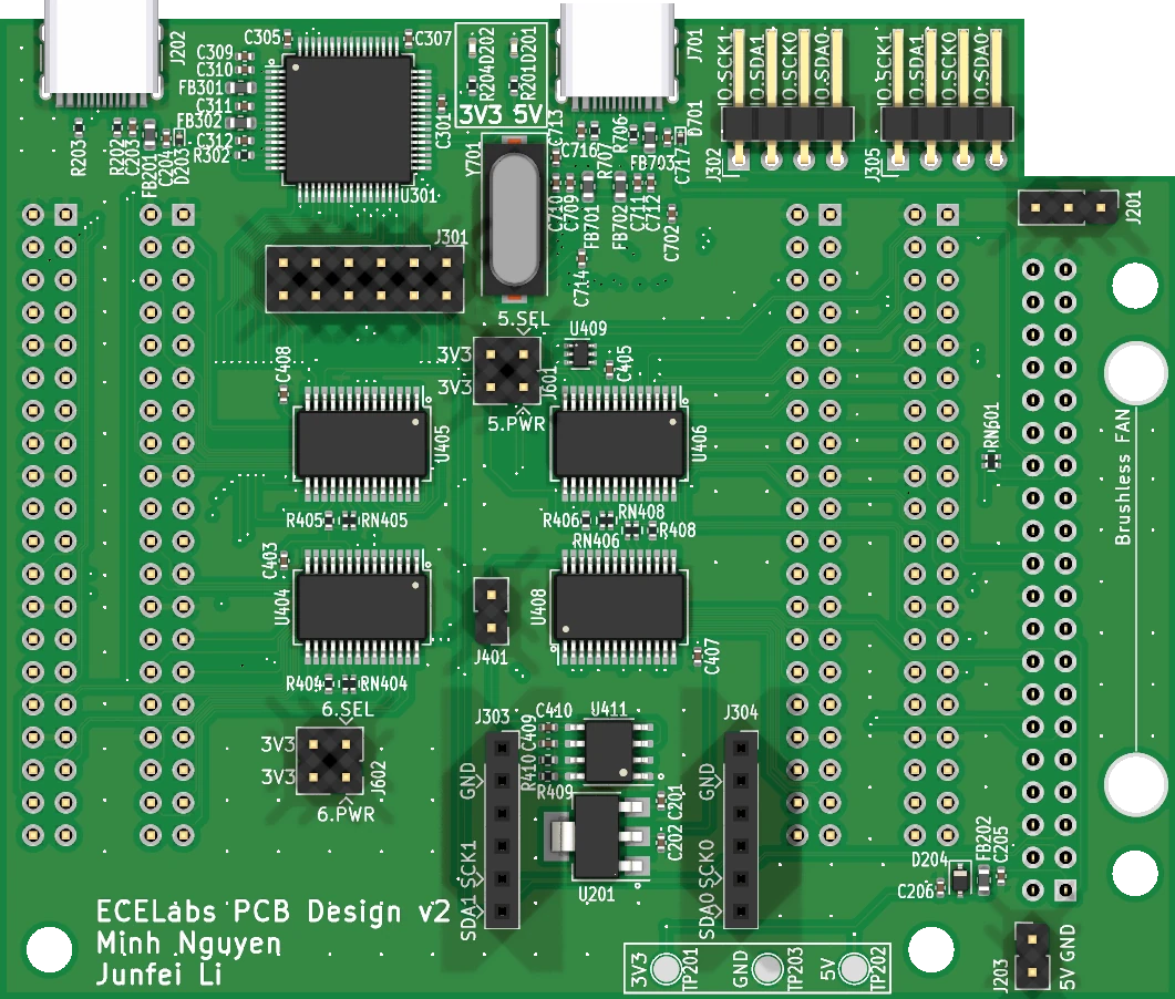
A four-layer carrier: a Raspberry Pi drives an iCE40 FPGA's pins through eight I2C expanders, at about half the first board's area. It went into the lab's stations.
- FT4232HLI2C buses
- 8 MCP23017I2C expanders
- Master select2x6 jumpers
- NE555Clock
- Raspberry Pi 4BSocket
91.4 × 76.2 mm4 copper layers139 footprints258 nets432 vias8 MCP23017 expanders
- Logic
- I/O
- Sensing
The problem
In ECE 270, students learn to use an FPGA and logic gates and to write SystemVerilog, on iCE40-HX8K FPGA boards. Each lab station joined one of those boards to a Raspberry Pi 4B with jumper wires. The carrier replaces the wires: in my README’s words, it uses “only 1 Pi4B to talk to read/write to FPGA ice40 pins”.
The FPGA board has about 103 I/O pins, far more than the Pi’s 40-pin header offers. I drew v2 from June to August 2023, after the first carrier of May.
How it works
Eight MCP23017 I/O expanders do the pin work. An I/O expander gives a processor 16 more pins over a serial bus, here I2C. The Pi masters two I2C buses to them, and an FT4232H USB chip can join either bus from a computer.
A second FT4232H connects to 32 of the FPGA’s output lines, and an NE555 timer makes a clock for the FPGA. An AZ1117 regulator makes 3.3 V from USB-C’s 5 V. Click a block to see what each part does.
ECELabs I2C carrier v2, block by block. Blocks: USB-C (“I2C USB”); FT4232H (I2C master over USB); 2×6 jumper header (joins the FTDI to each bus); NE555 (clock, CLK100); Raspberry Pi 4B (bus 0 and bus 1); 8 × MCP23017 (0x20 to 0x27); iCE40-HX8K board (about 103 pins); USB-C (“GPIO USB”); GPIO Stream (second FT4232H). USB-C to FT4232H; FT4232H to 2×6 jumper header, I2C; 2×6 jumper header to and from 8 × MCP23017, I2C; Raspberry Pi 4B to and from 8 × MCP23017, I2C; 8 × MCP23017 to and from iCE40-HX8K board; NE555 to iCE40-HX8K board; USB-C to GPIO Stream; iCE40-HX8K board to GPIO Stream, 32 lines.
Click a labeled block to see what it does.
The board, block by block
The Pi and the first FT4232H reach the FPGA's pins through eight expanders, and the second FT4232H taps its outputs. Click a block to see what it does.
In this layer
- USB-C and FT4232H An FT4232H, a USB chip with four serial ports, can master the same two I2C buses from a computer.
- 2×6 jumper header Shunts on a 2×6 header join the FT4232H to each I2C bus.
- NE555 An NE555 timer makes a clock, CLK100 on the schematic, for the FPGA.
- Raspberry Pi 4B The station's Pi plugs into the carrier and masters both I2C buses.
- 8 × MCP23017 Eight MCP23017 I/O expanders, chips that each give a processor 16 more pins over a serial bus.
- iCE40-HX8K board The lab's iCE40-HX8K board plugs into the carrier. Four 2×20 headers carry the expanders' lines to its pins.
- USB-C and GPIO Stream A second FT4232H, labeled “GPIO Stream” on the schematic, has its own USB-C port.
FT4232H: a second I2C master
An FT4232H, a USB chip with four serial ports, can master the same two I2C buses from a computer.
Why the Pi masters the bus
I first meant the FTDI chip to drive the expanders over USB. I chose the Pi's own I2C bus over it because, as my README records, the “pyftdi library processes the i2c bus very slow (<100Hz read/write)”. Its advice: “not to use the FTDI chip”.
Jumper header: joining the FTDI to a bus
Shunts on a 2×6 header join the FT4232H to each I2C bus.
The Pi stays on both buses either way, so the shunts only add a second master, as the drawing shows for bus 0.
Two masters for one I2C bus
Schematic of I2C bus 0 on the ECELabs I2C carrier. The bus lines IO.SCK0 and IO.SDA0 run to the clock and data pins of two MCP23017 expanders, U401 and U402, and to pins 28 and 27 of J603, the Raspberry Pi 4B header. RN601, two 10 kΩ resistors, pulls both lines up to 3.3 V. Jumper header J301 joins the bus to the FT4232HL chip U301: pins 5 and 6 join its ADBUS0 clock line, pins 7 and 8 its data line, on which ADBUS1 and ADBUS2 are tied together. U401 ties address pins A2, A1 and A0 to ground; U402 ties A2 and A1 to ground and A0 to 3.3 V. Connections: FTDI.SCK0 joins U301 ADBUS0, J301 5; FTDI.SDA0 joins U301 ADBUS1, U301 ADBUS2, J301 7; IO.SCK0 joins J301 6, RN601A, U401 SCL, J603 28, U402 SCL; IO.SDA0 joins J301 8, RN601B, U401 SDA, J603 27, U402 SDA; +3V3 joins RN601A, RN601B, U402 A0; GND joins U401 A2, U401 A1, U401 A0, U402 A2, U402 A1.
Bus 0 of the board's two I2C buses, with parts, pins and connections from the schematic's FTDI, GPIO Expansion and Pi4 sheets. The highlighted lines are the bus the expanders share. Bus 1, on the Pi's pins 3 and 5, carries the other six expanders, strapped to addresses 0x22 to 0x27.
- Shunts across J301 pins 5–6 and 7–8 join the FT4232HL to the bus as a second master, driven over USB. The Pi's pins are on the bus either way.
- RN601 pulls both lines up to 3.3 V. An I2C chip can only pull a line low, so the resistors bring it back high.
- Each MCP23017 takes its address from pins A2, A1 and A0. U401 ties all three low for 0x20; U402 ties A0 high for 0x21.
- My README later records that the FTDI route was too slow: with the pyftdi library it managed fewer than 100 reads and writes a second. The Pi became the master.
Bus 0 only; the schematic names the clock line SCK. Left out: RN301, the FTDI side's own 10 kΩ pull-ups; J302 and J304, headers on the same lines; the expanders' supply, reset and interrupt pins; and the rest of U301 and J603.
NE555: a clock for the FPGA
An NE555 timer makes a clock, CLK100 on the schematic, for the FPGA.
Where it goes
A jumper, J401, puts the clock on the FPGA's PB20 line.
Raspberry Pi 4B: the bus master
The station's Pi plugs into the carrier and masters both I2C buses.
Two buses
Bus 0, on header pins 27 and 28, reaches two expanders at addresses 0x20 and 0x21. Bus 1, on pins 3 and 5, reaches the other six, at 0x22 to 0x27.
Eight I2C expanders
Eight MCP23017 I/O expanders, chips that each give a processor 16 more pins over a serial bus.
The MCP23017 talks I2C, a two-wire bus on which each chip answers to its own address.
Addresses
Each chip's three address pins are tied high or low, which gives the eight addresses 0x20 to 0x27.
iCE40-HX8K board
The lab's iCE40-HX8K board plugs into the carrier. Four 2×20 headers carry the expanders' lines to its pins.
GPIO Stream: a second FT4232H
A second FT4232H, labeled “GPIO Stream” on the schematic, has its own USB-C port.
It connects to 32 of the FPGA's output lines: the left and right LED rows and two seven-segment digits.
Design decisions
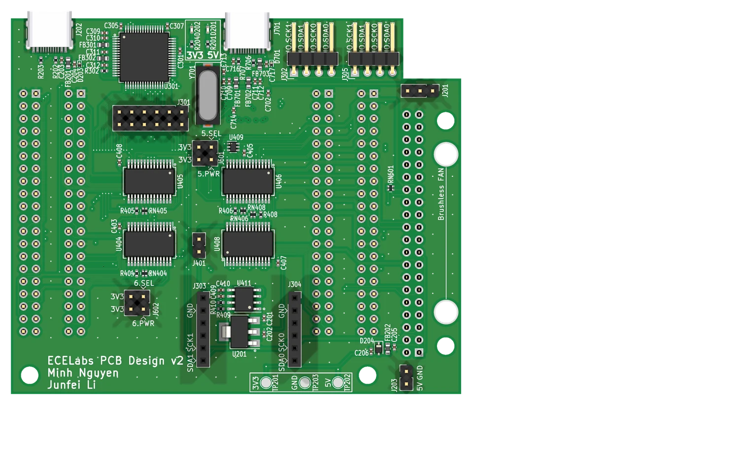
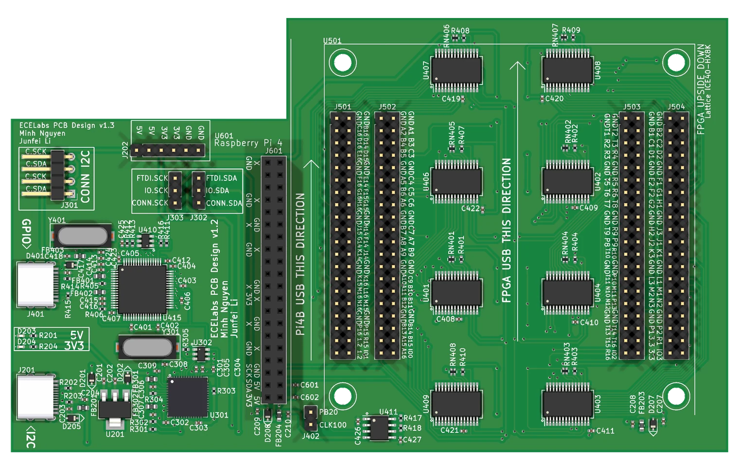
v2 is 91.4 × 76.2 mm, about half the area of the v1.3 board, on the same four layers. Why the Pi, not the FTDI chip, masters the expanders is in the FT4232H block above.
Results
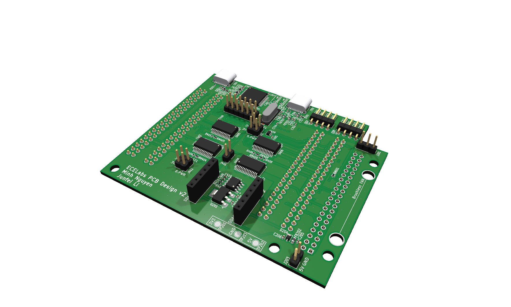
JLCPCB invoices show 10 assembled v2 boards ordered on 3 August 2023. By February 2024 the lab’s station diagram listed stations on v2 boards, beside the older v1.2 and v1.3. The lab ran 40 to 50 stations, each a Pi, an iCE40 board and one of my carriers.
I revised the layout as v2.1 in January 2024, on the same outline. I found no order for it.
No bus speed was measured: the 400 kHz in my README is the clock setting, not a result. The first carrier came before this board; the GPIO board and the software are the system’s other parts.
Explore the board
Pan, zoom and click any part. The schematic opens on the GPIO Expansion sheet, where the eight expanders are.
Loading the board layout.
Loading the schematic.
Credit
I designed the board.