ECE 270 FPGA breakout
ECELabs, Purdue ECE teaching labs
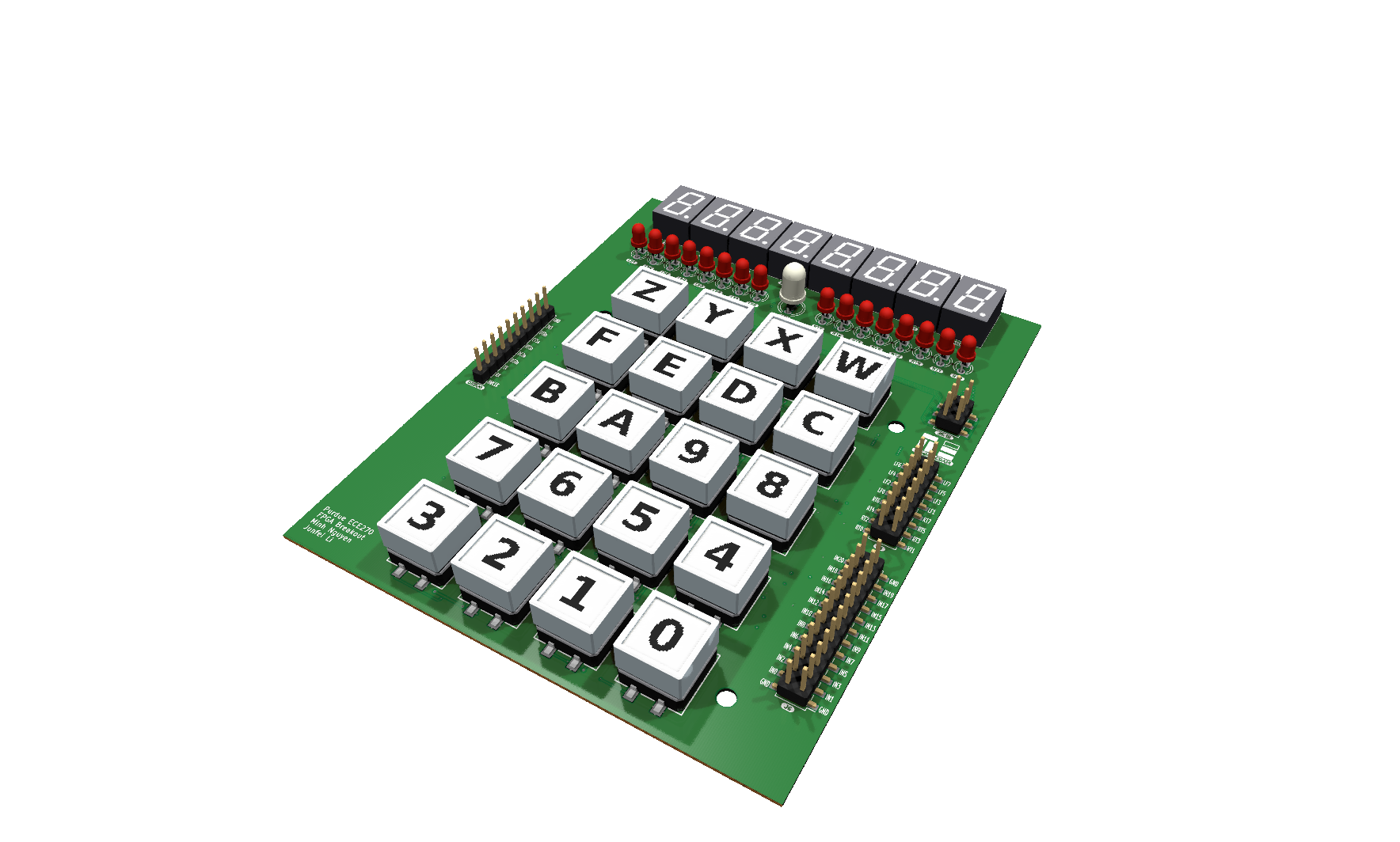
A push-button and display shield for the iCE40-HX8K evaluation board, on four layers. I designed two revisions and built both rounds of boards in spring 2024.
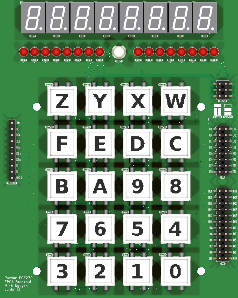
- 8 displaysSeven-segment
- RGB LED5 mm
- 16 red LEDs1.5 kΩ each
- 20 push buttonsStudent inputs
- 2x12 headerIN0 to IN20
99 × 124 mm4 copper layers247 footprints302 nets321 vias4 SN74HC14 chips
- Logic
- I/O
- Sensing
The problem
In ECE 270, students learn to use an FPGA and logic gates and to write SystemVerilog. A design needs inputs to press and outputs to watch. This board carries them for the lab’s iCE40-HX8K evaluation boards: 20 push buttons, eight seven-segment displays, 16 red LEDs and an RGB LED.
Four 2×20 headers on its back sit on the evaluation board. I started the design on 7 March 2024.
How it works
The board gives a student’s FPGA design 20 buttons to press, and eight seven-segment displays and 17 LEDs to watch. Each button passes through an RC filter and a Schmitt trigger on its way to the FPGA. The FPGA drives the displays and LEDs directly, through resistors. Click a block to see what each part does.
ECE 270 FPGA breakout, block by block. Blocks: 20 push buttons (100 kΩ pull-ups); RC filter (100 kΩ, 0.1 µF); SN74HC14 (Schmitt triggers); iCE40-HX8K board (through four 2×20 headers); 8 displays (seven-segment); 17 LEDs (16 red, 1 RGB). 20 push buttons to RC filter; RC filter to SN74HC14; SN74HC14 to iCE40-HX8K board; iCE40-HX8K board to 8 displays; iCE40-HX8K board to 17 LEDs.
Click a labeled block to see what it does.
The board, block by block
Each button runs through a filter and a trigger into the FPGA board, and the FPGA drives the displays and LEDs directly. Click a block to see what it does.
In this layer
- 20 push buttons Twenty push buttons, SW0 to SW19 on the silkscreen, are the inputs a student's design reads.
- RC filter A second 100 kΩ resistor and a 0.1 µF capacitor on each button line form an RC filter, a resistor and capacitor that smooth out fast changes.
- SN74HC14 Four SN74HC14 chips hold the Schmitt triggers, six to a chip. A Schmitt trigger is a gate that switches high and low at two different thresholds.
- iCE40-HX8K board The lab's iCE40-HX8K evaluation board. Four 2×20 headers on the back of my board sit on it.
- 8 displays Eight LTS-4301JR seven-segment displays, SS0 to SS7 on the silkscreen.
- 17 LEDs Sixteen red 3 mm LEDs in two banks of eight, LF0 to LF7 and RT0 to RT7, and one 5 mm RGB LED.
Push buttons: 20 inputs
Twenty push buttons, SW0 to SW19 on the silkscreen, are the inputs a student's design reads.
Each one pulls its line to ground when pressed, and a 100 kΩ resistor pulls it up to 3.3 V otherwise.
The caps
Each button wears a clear cap over a card with a black hex letter: 0 to F on the first sixteen, and W, X, Y and Z on the last four.
RC filter: one slow edge
A second 100 kΩ resistor and a 0.1 µF capacitor on each button line form an RC filter, a resistor and capacitor that smooth out fast changes.
A mechanical contact bounces, opening and closing several times in its first milliseconds, and the filter turns those bounces into one slow edge.
Schmitt triggers: one clean step
Four SN74HC14 chips hold the Schmitt triggers, six to a chip. A Schmitt trigger is a gate that switches high and low at two different thresholds.
It turns the filter's slow edge back into one clean step before the FPGA sees it.
Pressed reads 1
Each trigger also inverts, so a pressed button reads as 1 at the FPGA. A 1.5 kΩ resistor feeds each trigger.
iCE40-HX8K board: where it plugs in
The lab's iCE40-HX8K evaluation board. Four 2×20 headers on the back of my board sit on it.
Every button, display and LED line crosses those headers, along with 3.3 V and ground.
Seven-segment displays
Eight LTS-4301JR seven-segment displays, SS0 to SS7 on the silkscreen.
The FPGA drives each segment through its own 1.5 kΩ resistor, so the board needs no driver chip.
LEDs: two red banks and one RGB
Sixteen red 3 mm LEDs in two banks of eight, LF0 to LF7 and RT0 to RT7, and one 5 mm RGB LED.
The FPGA drives each red LED through its own 1.5 kΩ resistor, and the RGB LED through three 200 Ω resistors.
Bring-up
I built the boards in two rounds. In April 2024 I ordered 5 bare and 5 assembled v1 boards from JLCPCB, and my log records soldering them on 18 and 26 April.
I designed v2 from 29 April to 7 May and ordered 20 assembled boards on 8 May. My log records soldering and assembling them from 15 to 25 May. The log does not say what v1 got wrong, and the v2 layout is not in my archive, so the viewers show v1.
Results
No test of either revision is on record, so nothing on this page is measured. The last entry in my log is v2 assembly, on 25 May 2024. The I2C carrier, the GPIO board and the software are the lab’s other parts.
Explore the board
Pan, zoom and click any part. The schematic opens on the push-button sheet.
Loading the board layout.
Loading the schematic.
Credit
I designed both revisions, and soldered and assembled both rounds of boards. JLCPCB made the PCBs and assembled 25 of them.