ECELabs FPGA carrier, v1
ECELabs, Purdue ECE teaching labs
A first carrier that replaces jumper wires with eight I/O expanders between a Raspberry Pi 4B and an iCE40-HX8K FPGA. Its I2C line, reworked as v1.2 and v1.3, went into the lab.
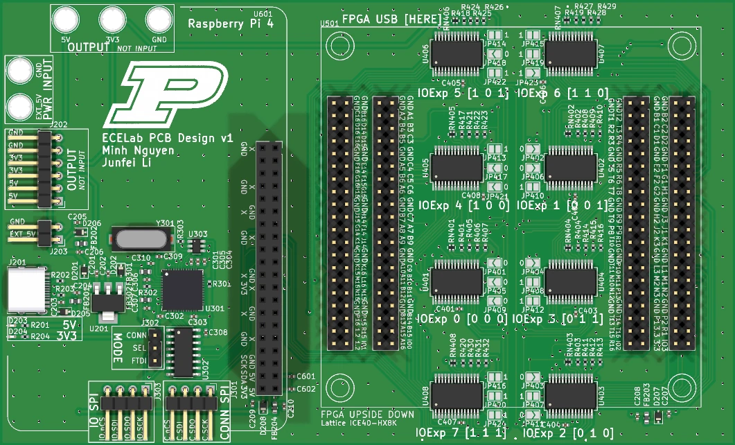
- FT232HQUSB bridge
- USB-C portPower and data
- AZ1117 LDO3.3 V rail
- SN74LVC157SPI master mux
- 8 MCP23S17SPI expanders
147.5 × 89.3 mm2 copper layers141 footprints265 nets434 vias24 solder jumpers
- Power
- I/O
- Sensing
The problem
In ECE 270, Purdue’s digital design course, students learn to use an FPGA and logic gates and to write SystemVerilog. An FPGA is a chip whose logic is set by the design loaded into it. In May 2023 each lab station joined a Raspberry Pi 4B to an iCE40-HX8K FPGA board with jumper wires.
In my README’s words, the aim was to make the station less “jumper wired”, with one Pi reading and writing about 103 FPGA pins. My plan gave the schematics three days, 15 to 17 May, and set 19 May as the deadline for ordering.
How it works
The Pi has too few pins for the FPGA’s 103, so eight I/O expanders reach them. An I/O expander is a chip that gives a processor 16 more pins over a serial bus, and this version’s expanders talk SPI. A jumper picks who drives that bus: the Pi, or an FT232H USB chip that lets a computer drive it directly, which we used mostly for debugging. Click a block to see what each part does.
ECELabs FPGA carrier v1, block by block. Blocks: USB-C port (power and data); AZ1117 (3.3 V regulator); FT232H (USB to SPI); SN74LVC157 (multiplexer, set by a jumper); External connector (SPI); Raspberry Pi 4B (SPI0); 8 × MCP23S17 (I/O expanders); iCE40-HX8K board (about 103 pins). USB-C port to FT232H, USB; USB-C port to AZ1117, 5 V; FT232H to SN74LVC157; External connector to SN74LVC157; SN74LVC157 to 8 × MCP23S17, SPI; Raspberry Pi 4B to 8 × MCP23S17, SPI; 8 × MCP23S17 to and from iCE40-HX8K board.
Click a labeled block to see what it does.
The board, block by block
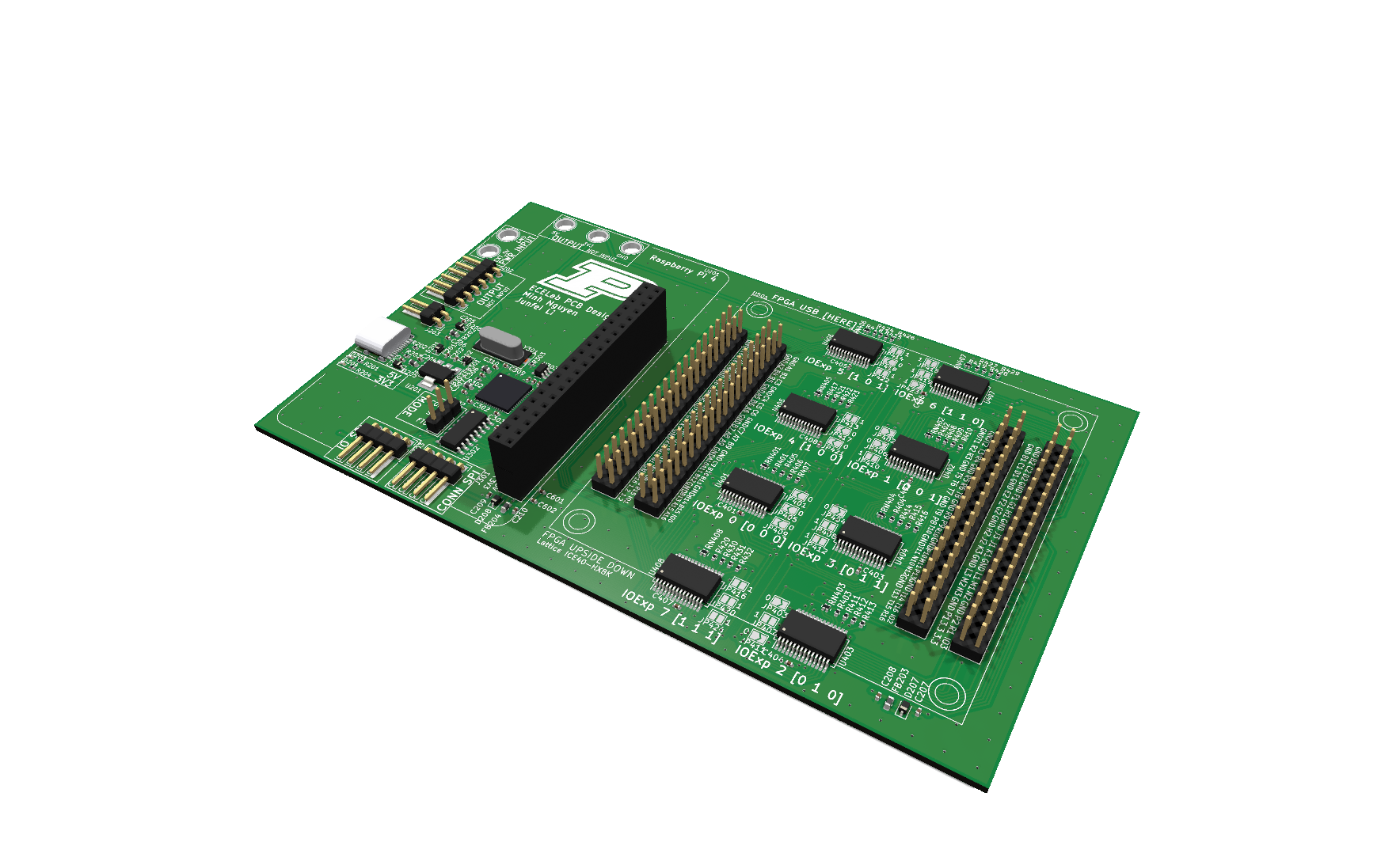
Power and the USB chip are at the left, and the expanders sit between the Pi and the FPGA board. Click a block to see what it does.
In this layer
- USB-C port and AZ1117 Power comes in on a USB-C port, and an AZ1117 regulator makes the 3.3 V rail.
- FT232H An FT232H, a USB-to-serial chip, lets a computer drive the expanders' SPI lines in place of the Pi. We used it mostly for debugging, since USB is easier to reach than the Pi.
- SN74LVC157 A multiplexer, a chip that passes one of two sets of inputs, puts either the FT232H or the Pi's connector on the shared SPI lines. A jumper on J302 picks which, so the two masters can be swapped.
- External connector A four-pin header that carries a clock, a chip select and both data lines to the multiplexer's second input.
- Raspberry Pi 4B The station's Pi mounts on the carrier and drives the shared SPI lines from its SPI0 pins.
- 8 × MCP23S17 Eight MCP23S17 I/O expanders, chips that each give a processor 16 more pins over a serial bus. The schematic symbol reads MCP23017, the I2C twin; its pins here are wired as the SPI part's.
- iCE40-HX8K board The lab's iCE40-HX8K breakout board mounts on the carrier, and the expanders reach about 103 of its pins.
Power: USB-C in, 3.3 V out
Power comes in on a USB-C port, and an AZ1117 regulator makes the 3.3 V rail.
Data
The same port carries USB data to the FT232H.
FT232H: a way in from a computer
An FT232H, a USB-to-serial chip, lets a computer drive the expanders' SPI lines in place of the Pi. We used it mostly for debugging, since USB is easier to reach than the Pi.
Beside it
A 93LC56 EEPROM, a small memory chip, and a 12 MHz crystal support it.
SN74LVC157: picking the second master
A multiplexer, a chip that passes one of two sets of inputs, puts either the FT232H or the Pi's connector on the shared SPI lines. A jumper on J302 picks which, so the two masters can be swapped.
Set by a jumper
A three-pin header sets its select pin to 3.3 V or ground, and a shunt picks the side.
External connector
A four-pin header that carries a clock, a chip select and both data lines to the multiplexer's second input.
Raspberry Pi 4B: the station's computer
The station's Pi mounts on the carrier and drives the shared SPI lines from its SPI0 pins.
Eight SPI expanders
Eight MCP23S17 I/O expanders, chips that each give a processor 16 more pins over a serial bus. The schematic symbol reads MCP23017, the I2C twin; its pins here are wired as the SPI part's.
Together they reach the FPGA's pins, about 103, far more than the Pi has.
SPI
The MCP23S17 talks SPI: a four-wire bus with a clock, a line each way for data and a chip select.
Addresses
All eight share one chip select, so each needs an address of its own. 24 solder jumpers, three per chip, set them, as the drawing shows.
Setting an expander's address
Schematic of expander U404, an MCP23S17T-E/SS, on the ECELabs FPGA carrier v1. Its chip select, clock, data-in and data-out pins go to the shared SPI lines IO.~CS, IO.SCK, IO.SDO and IO.SDI. Each of its address pins A2, A1 and A0 has a 10 kΩ pull-down to ground, R414, R415 and R416, and a solder jumper to 3.3 V, JP404, JP408 and JP412. JP404 is open and JP408 and JP412 are bridged, so the address is 011. Connections: A2 joins U404 A2, JP404, R414; A1 joins U404 A1, JP408, R415; A0 joins U404 A0, JP412, R416; IO.~CS joins U404 CS; IO.SCK joins U404 SCK; IO.SDO joins U404 SI; IO.SDI joins U404 SO; +3V3 joins JP404, JP408, JP412; GND joins R414, R415, R416.
One of the eight MCP23S17 expanders, with parts, values and connections from the schematic's GPIO Expander 3 block. The highlighted nets are its three address pins.
- All eight expanders share these four SPI lines, chip select included. With hardware addressing on, each one answers only to messages that carry its own address.
- Each address pin has a 10 kΩ pull-down to ground and a solder jumper to 3.3 V. An open jumper reads 0 and a bridged one reads 1.
- U404's jumpers set A2, A1 and A0 to 011. Across the board, 24 jumpers give the eight expanders the addresses 000 to 111.
As built, JP404 is open and JP408 and JP412 are bridged. Left out: the other seven expanders, U404's supply, reset, interrupt and port pins, and their parts.
iCE40-HX8K board
The lab's iCE40-HX8K breakout board mounts on the carrier, and the expanders reach about 103 of its pins.
Design decisions
I drew two versions of this board in May 2023, one with I2C expanders and this one with SPI. I proposed finishing the I2C version first, “since it’s the current system and it’s best to keep what’s working”. SPI, I wrote, “needs more time to test”. It cost speed: I had listed the SPI version as the one aimed at “faster speed through SPI bus”.
Results
I found no order for this SPI version and no record of a build, so nothing on it was measured. A JLCPCB invoice shows 2 assembled and 3 bare “ECELab_v1” boards ordered on 24 May 2023, five days before I finished the SPI design.
The I2C line went on. Its four-layer v1.2 and v1.3 boards kept this outline and were in the lab’s stations by February 2024. The I2C carrier then shrank the design to about half the area. The GPIO board and the software are the system’s other parts.
Explore the board
Pan, zoom and click any part. The schematic opens on the GPIO Expansion sheet, where the eight expanders are.
Loading the board layout.
Loading the schematic.
Credit
I designed both versions of the board.