ROV X14 power conversion board
Purdue IEEE ROV
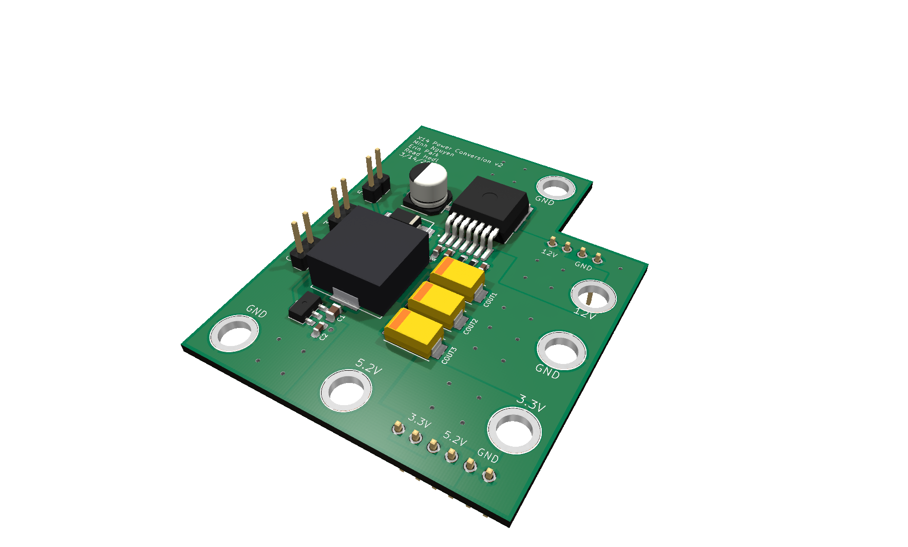
A step-down board that made the 2021-22 ROV's 5.2 V and 3.3 V rails from 12 V. Its second revision steadied the 5.2 V rail.
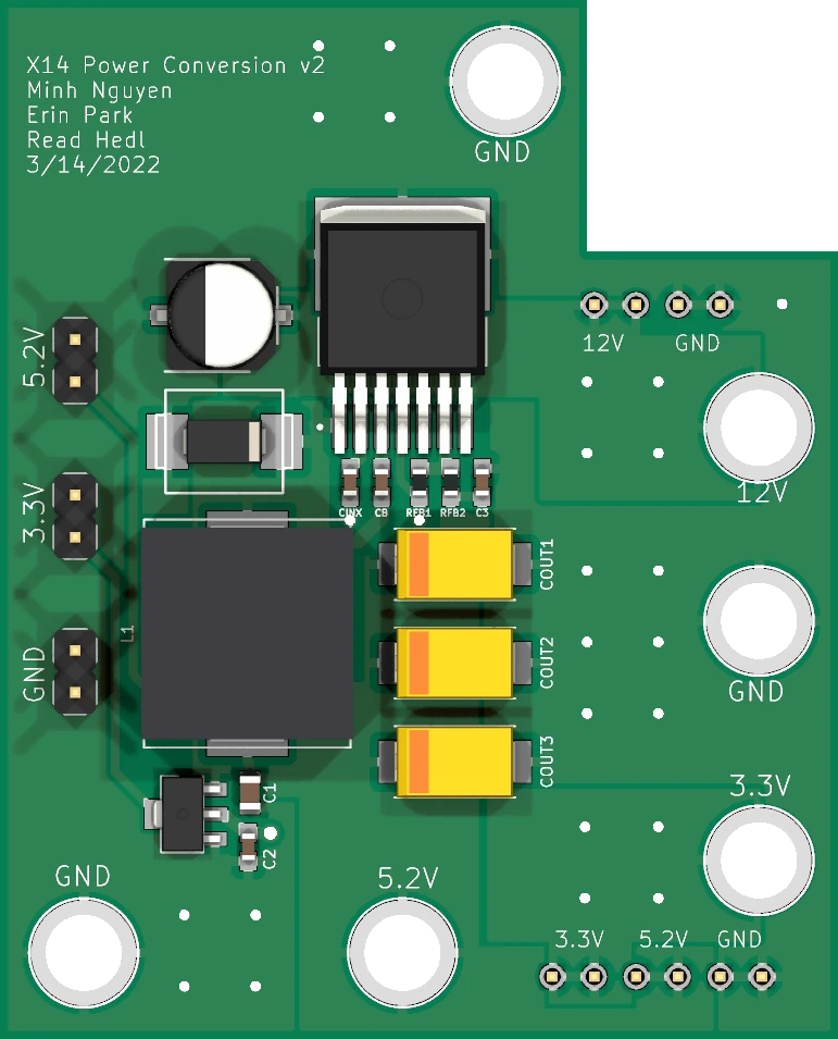
- LM2678 buck12 V to 5.2 V
- AZ1117 LDO5.2 V to 3.3 V
- Buck inductor22 µH
- Output caps5.2 V rail
- To DistributionPower in, out
50.8 × 62.9 mm2 copper layers25 footprints7 nets
- Power
- I/O
The problem
The team’s 2021-22 vehicle needed 5.2 V and 3.3 V, and its power box had only 48 V and 12 V. My board had to make 5.2 V, rated 3 A, and 3.3 V, rated 1 A, from the 12 V. The 5.2 V rail fed the Raspberry Pi. The 3.3 V rail fed the ESC controller boards, which command the thrusters’ speed controllers.
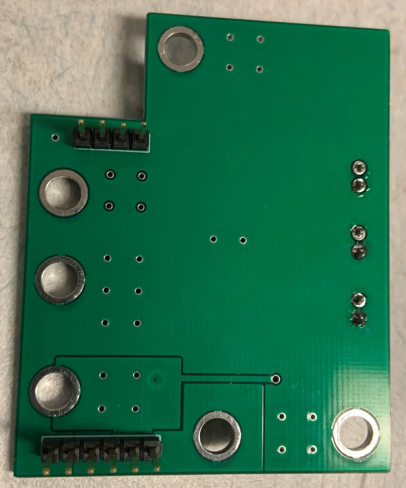
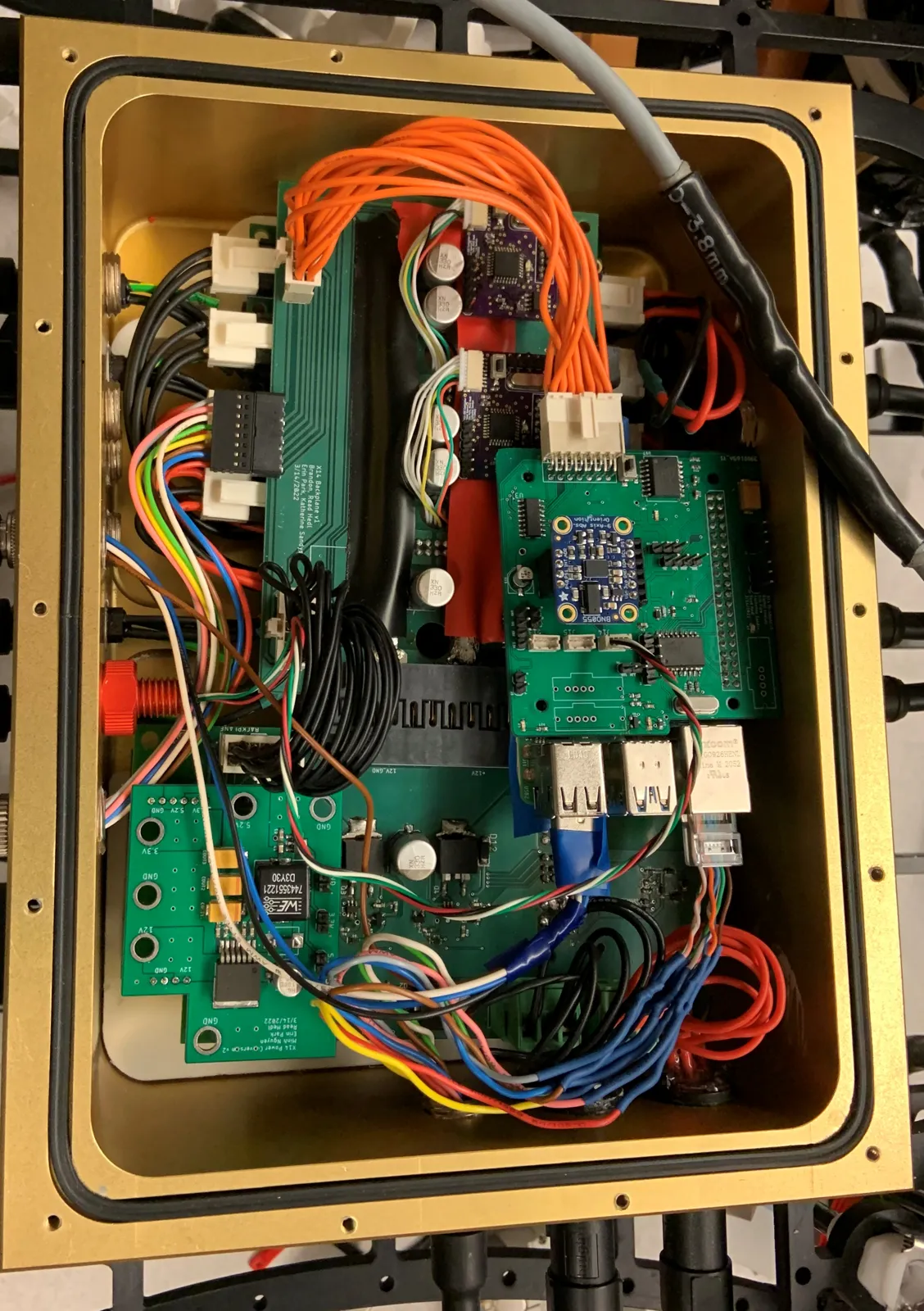
The board sat on top of the Distribution board, joined to it by two connectors. It had to stay short enough to leave that board’s other connectors clear.
How it works
The board steps 12 V down in two stages and carries no data. A buck converter, a switching regulator that steps voltage down, makes 5.2 V. An LDO, a linear regulator, makes 3.3 V from that rail. Both rails return to the Distribution board, and the Backplane carries them on.
Click a block to see what it does and why I designed it that way.
X14 Conversion board, block by block. Blocks: From Distribution (12 V in); Buck converter (LM2678S-ADJ); Output filter (22 µH, 3 × 150 µF); To Distribution (5.2 V and 3.3 V out); Test points (12 V, 5.2 V, 3.3 V); Feedback (1 kΩ and 3.32 kΩ); LDO (AZ1117, 3.3 V). From Distribution to Buck converter, 12 V; Buck converter to Output filter; Output filter to To Distribution, 5.2 V; Output filter to LDO, 5.2 V; LDO to To Distribution, 3.3 V; Feedback to Buck converter, FB.
Click a labeled block to see what it does and why.
The board, block by block
12 V comes in at the left, and both rails leave at the right. Click a block to see what it does and why I designed it that way.
In this layer
- From Distribution 12 V from the Distribution board, through its Schottky diodes, on the connector at the top of the board.
- Buck converter An LM2678S-ADJ buck converter makes 5.2 V. It switches its input on and off quickly, and the output filter smooths the pulses.
- Output filter A 22 µH inductor and three 150 µF capacitors smooth the switching pulses into a steady 5.2 V.
- Feedback Two resistors, 1 kΩ and 3.32 kΩ, feed a fraction of the output back to the chip's 1.21 V reference, which sets the rail to 5.2 V.
- LDO An AZ1117 LDO, a linear regulator, makes 3.3 V, rated 1 A, from the 5.2 V rail.
- Test points Probe points for 12 V, 5.2 V, 3.3 V and ground, for checks on the bench.
- To Distribution 5.2 V, rated 3 A, and 3.3 V, rated 1 A, return to the Distribution board on the connector at the bottom of the board.
From Distribution: 12 V in
12 V from the Distribution board, through its Schottky diodes, on the connector at the top of the board.
The two connectors are the board's only support, so they were picked with almost the same pin count, 4 and 6.
At bring-up
v1 covered the Distribution board's connectors, so “we have to cut the end of the board and eliminate the test terminals”. v2 is shorter.
Buck converter: 12 V to 5.2 V
An LM2678S-ADJ buck converter makes 5.2 V. It switches its input on and off quickly, and the output filter smooths the pulses.
I chose its 7-pin TO-263 package because it is “Easy to solder”.
The switch node
The switch node swings between about 0 V and the input voltage every cycle, so the larger its loop, the more noise it radiates. An alumni reviewer called my first layout a “Bad noise/EMI layout”. I placed the LM2678, the diode and the inductor “as close together as possible” on one copper polygon.
What it cost
Room to solder. My notes list “Small components for the buck converters are placed very close together” as a mistake.
At bring-up
I ordered the catch diode, which carries the inductor current while the switch is off, in a package too small for its pads, so I built up solder on its leads to reach them. I also soldered it in backwards once, then fixed it. The 10 nF bootstrap capacitor, which lets the chip drive its own switch, was left off the order.
How it makes 5.2 V and 3.3 V
Schematic of the X14 Conversion board. 12 V from the Distribution board connector feeds the input capacitors and the LM2678S-ADJ buck converter U1. U1's switch node SW joins the bootstrap capacitor CB, the Schottky diode D1 and the inductor L1. L1 and three 150 µF capacitors make the 5.2 V rail, which a 3.32 kΩ and 1 kΩ divider feeds back to U1's FB pin. The 5.2 V rail feeds the AZ1117CR-3.3 regulator, which makes 3.3 V. Both rails return to the connector. Connections: 12V joins CONN 12V, CIN +, CINX, U1 VIN; CB joins U1 CB, CB; SW joins U1 SW, CB, D1 K, L1; 5.2V joins CONN 5.2V, L1, COUT1 +, COUT2 +, COUT3 +, RFB2, LDO IN, C1, C3; FB joins U1 FB, RFB2, RFB1; 3.3V joins CONN 3.3V, LDO OUT, C2; GND joins CONN GND, CIN -, CINX, U1 GND, D1 A, COUT1 -, COUT2 -, COUT3 -, RFB1, LDO GND, C1, C3, C2.
The board's circuit, with its connections taken from the board file. The tinted area is everything on the switch node.
- U1's switch, D1, L1 and CB all meet at the switch node, SW. I placed them as close together as possible, on a copper polygon, to keep this noisy loop small.
- L1 and three 150 µF tantalum capacitors smooth the switched voltage into a steady 5.2 V. v1 used a 15 µH inductor and smaller capacitors, and its rail spiked.
- RFB2 and RFB1 divide 5.2 V down to the 1.21 V that U1 holds at FB: 1.21 V × (1 + 3.32 ÷ 1) is about 5.2 V.
- The AZ1117 takes 5.2 V, not 12 V, so it drops 1.9 V instead of 8.7 V and turns less power into heat.
CONN stands for both connectors to the Distribution board. L1 is 22 µH, as built. The 3 A and 1 A are ratings, not load tests.
Output filter: a steadier 5.2 V
A 22 µH inductor and three 150 µF capacitors smooth the switching pulses into a steady 5.2 V.
A larger inductor slows how fast its current can change, and more capacitance absorbs what is left, so the rail moves less.
v1 to v2
I chose 22 µH and three 150 µF capacitors over v1's 15 µH and two 100 µF plus one 150 µF, because v1's output spiked. On v2 the “output stays right at 5.2V”.
Numbers
| Part | v1 | v2 |
|---|---|---|
| Inductor | 15 µH | 22 µH |
| Output capacitors | 2 × 100 µF, 1 × 150 µF | 3 × 150 µF |
Feedback: why 5.2 V
Two resistors, 1 kΩ and 3.32 kΩ, feed a fraction of the output back to the chip's 1.21 V reference, which sets the rail to 5.2 V.
I chose the adjustable LM2678S-ADJ over the fixed 5 V LM2678S-5.0 because the Raspberry Pi throttles itself when its supply is not above 5 V.
What it cost
Two feedback resistors and a calculation from the datasheet.
LDO: 3.3 V from the 5.2 V rail
An AZ1117 LDO, a linear regulator, makes 3.3 V, rated 1 A, from the 5.2 V rail.
An LDO turns the voltage it drops into heat: from 5.2 V it drops 1.9 V, where from 12 V it would drop 8.7 V.
Why this part
A teammate recommended the AZ1117, and it is a newer version of the regulator on the previous year's board.
Test points
Probe points for 12 V, 5.2 V, 3.3 V and ground, for checks on the bench.
At bring-up
The test points were too small to probe, and no LED showed that the board had power.
Carried forward
The X15 Conversion board, which a teammate drew from mine, added LEDs for 12 V, 5.2 V and 3.3 V.
To Distribution: the rails go out
5.2 V, rated 3 A, and 3.3 V, rated 1 A, return to the Distribution board on the connector at the bottom of the board.
The Backplane carries them on: 5.2 V to the Raspberry Pi, and 3.3 V to the ESC controller boards.
No data
The board carries no data signal: “There's no data signal, just the power sources getting converted into different voltages.”
Power path
Blocks: Tether (from the surface); Distribution board; Power brick boards (two boards); Conversion board (LM2678 and AZ1117); Backplane (carries the rails to the boards); Raspberry Pi (through the Pi Shield); ESC controllers; ESCs (Lumenier).
- Tether to Distribution board: 48 V, up to 30 A.
- Distribution board to Power brick boards: 48 V.
- Power brick boards to Distribution board: 12 V.
- Distribution board to Conversion board: 12 V.
- Conversion board to Distribution board: 5.2 V 3 A, 3.3 V 1 A.
- Distribution board to Backplane: 12 V, 3.3 V, 5.2 V.
- Backplane to Raspberry Pi: 5.2 V.
- Backplane to ESC controllers: 3.3 V.
- Backplane to ESCs: 12 V.
What I designed: Conversion board.
Design decisions
I wrote down the reasons for each choice in my design documentation, and alumni reviewers pushed on the layout.
The choice that shaped the whole board came first. The team now sent it 12 V instead of 48 V, so I chose one buck converter chip over last year’s buck controller driving a separate MOSFET. In my notes: “With simpler functions, X14 Power Conversion is smaller in size than last year’s.” It cost input range: last year’s board took 12 to 48 V, and this one takes “a max of 15V”.
The other choices are in their blocks above: the feedback that sets 5.2 V, the switch node and the output filter.
Bring-up
My first build, v1, went wrong in fit, ordering and assembly. I soldered the large parts first, which left the small ones “hard to solder”. v2 shortened the board, dropped the screw terminals and changed the output filter. Each fix is in its block above.
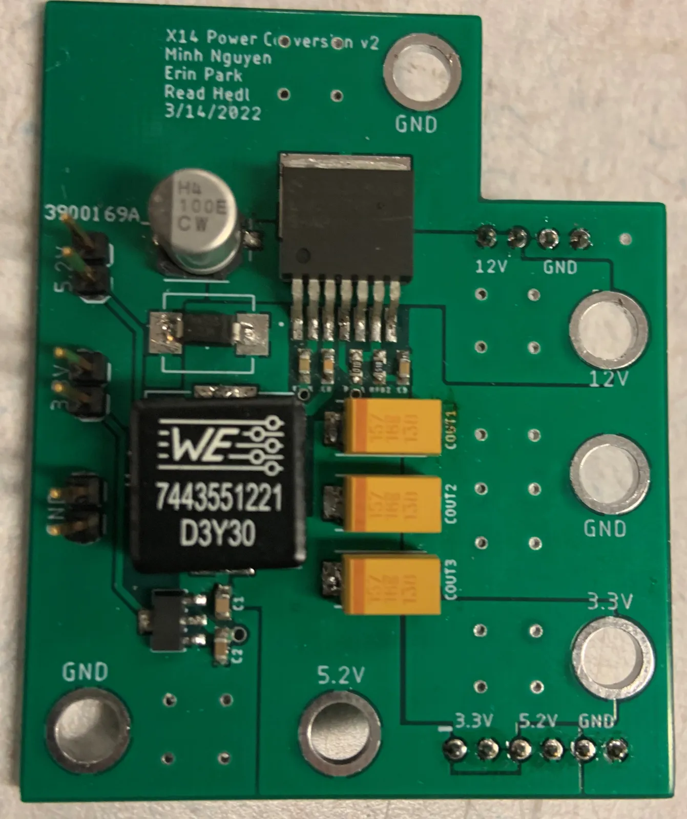
Results
No load test of the board is on record, so the 3 A and 1 A figures are ratings, not measurements. My notes record ripple on the 5.2 V rail “of around 0.04V or 40mV” peak to peak, without the method, load or revision.
The team placed 10th of 20 in-person teams in the Explorer class at the 2022 MATE ROV World Championship (score sheet). A teammate carried the board into X15 on the same outline, and X16 moved its job onto the Power Slab.
Explore the board
Pan, zoom and click any part. The views follow each other.
Loading the board layout.
Loading the schematic.
Credit
I designed the board and wrote its documentation; alumni reviewers critiqued the schematic and layout, and a teammate recommended the AZ1117.